
Datasheet


MAX1444
10-Bit, 40Msps, 3.0V, Low-Power
ADC with Internal Reference
______________________________________________________________________________________ 17
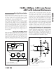
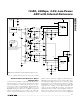
Unbuffered External Reference Drives
Multiple ADCs
Connecting each REFIN to analog ground disables the
internal reference of each device, allowing the internal
reference ladders to be driven directly by a set of exter-
nal reference sources. Followed by a 10Hz lowpass fil-
ter and precision voltage-divider (Figure 11), the
MAX6066 generates a DC level of 2.500V. The buffered
outputs of this divider are set to 2.0V, 1.5V, and 1.0V,
with an accuracy that depends on the tolerance of the
divider resistors. The three voltages are buffered by the
MAX4252, which provides low noise and low DC offset.
The individual voltage followers are connected to 10Hz
lowpass filters, which filter both the reference voltage
and amplifier noise to a level of 3nV/√Hz. The 2.0V and
1.0V reference voltages set the differential full-scale
range of the associated ADCs at 2V
P-P
. The 2.0V and
1.0V buffers drive the ADC’s internal ladder resistances
between them. Note that the common power supply for
all active components removes any concern regarding
REFOUT
29
N.C.
REFIN
31
REFP
32
REFN
1
COM
2
0.1
μ
F
0.1
μ
F
0.1
μ
F
330
μ
F
6V
330
μ
F
6V
330
μ
F
6V
10
μ
F
6V
11
4
3
2
3
1
2
1
MAX1444
N = 1
MAX6066
1/4 MAX4252
REFOUT
29
N.C.
REFIN
31
REFP
32
REFN
1
COM
2
0.1
μ
F
0.1
μ
F
0.1
μ
F
MAX1444
N = 32
47
Ω
2.0V AT 8mA
1.47k
Ω
21.5k
Ω
3.3V
1
μ
F
21.5k
Ω
21.5k
Ω
21.5k
Ω
21.5k
Ω
NOTE: ONE FRONT-END REFERENCE CIRCUIT DESIGN MAY BE USED WITH UP TO 32 ADCs.
2.2
μ
F
10V
0.1
μ
F
0.1
μ
F
3.3V
2.0V
10
μ
F
6V
11
4
5
6
7
1/4 MAX4252
47
Ω
1.5V AT 0mA
1.47k
Ω
3.3V
10
μ
F
6V
11
4
10
9
8
1/4 MAX4252
47
Ω
1.0V AT -8mA
1.47k
Ω
3.3V
3.3V
MAX4254 POWER-SUPPLY BYPASSING.
PLACE CAPACITOR AS CLOSE AS
POSSIBLE TO THE OP AMP.
0.1
μ
F
1.5V
1.0V
Figure 11. Unbuffered External Reference Drives Up to 32 ADCs