
Datasheet


MAX1407/MAX1408/MAX1409/MAX1414
Low-Power, 16-Bit Multichannel DAS with
Internal Reference,10-Bit DACs, and RTC
4 _______________________________________________________________________________________
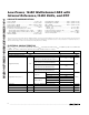
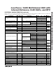
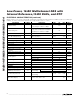
ELECTRICAL CHARACTERISTICS (continued)
(DV
DD
= AV
DD
= +2.7V to 3.6V, 4.7µF at REF, internal V
REF
, 18nF between CPLL and AV
DD
, 32.768kHz crystal across CLKIN and
CLKOUT, T
A
= T
MIN
to T
MAX
, unless otherwise noted. Typical values are at T
A
= +25°C.)
PARAMETER SYMBOL CONDITIONS MIN TYP MAX U N I T S
Output Slew Rate
010hex to 3FFhex and 3FFhex to 010hex
cod e sw i ng , R
L
= 12kΩ , C
L
= 200p F
18.0 V/ms
Output Settling Time
To ±1/2 LSB (at 10-bit accuracy) of full-
scale with code transition from 010hex
to 3FFhex, R
L
= 12kΩ, C
L
= 200pF
65 µs
Turn-On Time 100 µs
OUT1, OUT2 Output Range No Load (Note 4) 0.05
AV
DD
- 0.2
V
EXTERNAL REFERENCE (internal reference powered down)
Input Voltage Range 1.25 ±0.10 V
Input Resistance 540 kΩ
Input Current 2.3 µA
INTERNAL REFERENCE (AV
DD
= 3V, unless otherwise noted)
Output Voltage T
A
= +25°C 1.225 1.25 1.275 V
Output Voltage Temperature
Coefficient
18 p p m /° C
Output Short-Circuit Current 3.4 mA
Line Regulation ∆V
RE F
/∆V
DD
2.7<AV
DD
<3.6V 80 µV/V
I
SOURCE
= 0µA to 500µA, T
A
= +25°C1
Load Regulation
I
SINK
= 0µA to 50µA, T
A
= +25°C2
µV/µA
0.1Hz to 10Hz 40
Noise Voltage e
OUT
10Hz to 10kHz 400
µVp-p
Power-Supply Rejection Ratio ±100mV, f = 120Hz 70 dB
Turn-On Time 3ms
µP RESET
Supply Voltage Range For valid RESET 1 3.6 V
Bit VM = 1 1.800 1.865 1.930
RESET Trip Threshold Low V
TH
AV
DD
falling
Bit VM = 0 2.70 2.75 2.80
V
Low AV
DD
Trip Threshold
For Normal, Idle, and Standby modes,
AV
DD
falling
2.70 2.75 2.80 V
RESET Output Low Voltage
(Open-Drain Output)
I
SINK
= 1mA, AV
DD
= 1.8V 0.4 V