
Datasheet


MAX1407/MAX1408/MAX1409/MAX1414
Low-Power, 16-Bit Multichannel DAS with
Internal Reference,10-Bit DACs, and RTC
______________________________________________________________________________________ 35
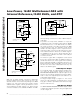
REFE: Internal Reference Power Enable. When REFE is
set to 1, the internal reference is powered up. When
REFE is set to 0, the internal reference is powered down
allowing an external reference to be connected to REF.
ADCE: ADC Power Enable. When ADCE is set to 1, the
ADC is powered up. When ADCE is set to 0, the ADC is
powered down.
BUFE: ADC Input Buffer Power Enable. A logic 1
enables the power-up of the ADC input buffers, while a
logic 0 powers-down the buffers.
MUXE: Multiplexer enable. A logic 0 disables the multi-
plexer outputs while a logic 1 enables them.
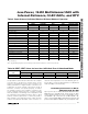
Power-Control Registers
Table 8 shows the bit values of some key registers in
different power modes under various conditions. Use
this as a quick reference when programming the
MAX1407/MAX1408/MAX1409/MAX1414 family.
Table 8. Related Bit Values During Specified Mode
CIRCUIT BLOCK BIT INITIAL POWER-UP SLEEP STANDBY IDLE RUN WAKE-UP EVENT
32kHz Oscillator CH 0 (oscillator is on) N/A N/A N/A N/A N/A
RTC CH 0 (RTC is on) N/A N/A N/A N/A N/A
Low V
DD
Voltage
Monitor (2.7V)
LVDE
1 (2.7V monitor is
on)
1 if VM = 0
0 if VM = 1
111 1
RESET Voltage
Monitor (1.8V)
LSDE
0 (1.8V monitor is
off)
0 if VM = 0
1 if VM = 1
0 if VM = 0
1 if VM = 1
0 if VM = 0
1 if VM = 1
0 if VM = 0
1 if VM = 1
N/A
Reset Bit RST 1 (RESET asserted) N/A N/A N/A N/A N/A
Low V
DD
Status Bit LVD
1 (low V
DD
)
N/A N/A N/A N/A N/A
Voltage-Monitor
Threshold Selection
VM 0 (select 2.7V) N/A N/A N/A N/A N/A
Bias Circuit BIASE
Biase = 1 (biase
circuit is on)
0111 1
PLL PLLE 1 (PLL is on) 0 1 1 1 1
PLL Output PLLE 1 (FOUT is enabled) 0 1 1 1 1
SHDN Output SHDE 1 ( S HD N p i n = hi g h) 0111 1
DAC1 DA1E 0 0 0 1 1 N/A
DAC2 DA2E 0 0 0 1 1 N/A
ADC MUX
MUX
0 0 0 1 1 N/A
Bandgap Reference REFE 0 0 0 1 1 N/A
Signal-Detect
Comparator
SDCE 0 0 0 1 1 N/A
ADC Buffers BUFE 0 0 0 0 1 N/A
ADC
ADC
0 0 0 0 1 N/A
N/A: Programming the part into these modes would not alter the content of the corresponding bit.
POWER1 REGISTER (11000)
FIRST BIT (MSB) (LSB)
NAME REFE ADCE BUFE MUXE DA1E DA2E ——
DEFAULT 00000000