
Datasheet


MAX1407/MAX1408/MAX1409/MAX1414
Low-Power, 16-Bit Multichannel DAS with
Internal Reference,10-Bit DACs, and RTC
_______________________________________________________________________________________ 3
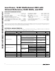
ELECTRICAL CHARACTERISTICS (continued)
(DV
DD
= AV
DD
= +2.7V to 3.6V, 4.7µF at REF, internal V
REF
, 18nF between CPLL and AV
DD
, 32.768kHz crystal across CLKIN and
CLKOUT, T
A
= T
MIN
to T
MAX
, unless otherwise noted. Typical values are at T
A
= +25°C.)
PARAMETER SYMBOL CONDITIONS MIN TYP MAX U N I T S
1/3
1PGA Gain See PGA Gain section
2
V/V
Power-Supply Rejection Ratio Gain = 1, unipolar and buffered mode 70 dB
RATE bit = 0 30
Output Update Rate
Continuous
conversion
RATE bit = 1 60
Hz
Turn-On Time Excluding reference 50 µs
SIGNAL DETECT COMPARATOR
MAX1407/MAX1408/MAX1409 -10 0 10
Differential Input-Detection
Threshold Voltage
MAX1414 44 50 56
mV
Common-Mode Input Voltage
0 0.8 V
Turn-On Time 10 µs
ANALOG INPUTS
ADC gain = 1 0 V
REF
ADC gain = 2 0 V
REF/2
Unipolar mode
ADC gain = 1/3 0 AV
DD
ADC gain = 1 -V
REF
V
REF
ADC gain = 2 -V
REF/2
V
REF/2
Differential Input Voltage Range
Bipolar mode
ADC gain = 1/3 -AV
DD
AV
DD
V
Unbuffered -0.05 AV
DD
Absolute Input Voltage Range
Buffered 0.05 1.40
V
Unbuffered AGND AV
DD
Common-Mode Input Voltage
Range
Buffered 0.05 1.40
V
Common-Mode Rejection Ratio Gain = 1, unipolar and buffered mode 90 dB
30Hz data rate 15.360
Input Sampling Rate FOUT = 2.4576MHz
60Hz data rate 30.720
kHz
Input Current Buffered mode ±0.5 nA
Input Capacitance 15 pF
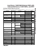
F O R C E- SEN SE D A C ( al l m easur em ents m ad e w i th FB1( 2) shor ted to O U T1( 2) , unl ess other w i se noted ) .
( M AX 1407/M AX 1409/M AX 1414 onl y)
Resolution 10 Bits
Differential Nonlinearity Guaranteed monotonic (Note 2) ±1.0 LSB
Integral Nonlinearity (Note 2) ±1.0 LSB
Offset Error (Note 3) ±20 mV
Offset Drift ±5 µV/°C
Gain Error Excludes offset and reference drift 3.6 mV
Gain Drift Excludes offset and reference drift 10 ppm/°C
Line Regulation 190 µV/V
Current into FB1(2) ±0.5 nA