
Datasheet


MAX1407/MAX1408/MAX1409/MAX1414
Low-Power, 16-Bit Multichannel DAS with
Internal Reference,10-Bit DACs, and RTC
28 ______________________________________________________________________________________
The Offset register contains the 16-bit result from the
most recently completed ADC offset calibration. The
data format is two’s complement and is subtracted from
the filter output before writing to the Data register. After
power-up, the Offset register contains all zeros.
Each change in ambient operating condition (power
supply and temperature), PGA gain, bipolar/unipolar
input range, buffered/unbuffered mode, or conversion
speed requires an offset calibration. The offset for a
given ADC configuration can be read and stored by the
µP to avoid ADC recalibration. When returning to an
ADC configuration where the offset was stored, write
back the stored offset to the Offset register. The stored
offset stays valid as long as the ambient operating con-
dition remains unchanged (within ±20°C).
Force Sense DAC Registers
(MAX1407/MAX1409/MAX1414 only)
Writing to the DAC1 register updates the output of
DAC1. Writing to the DAC2 register updates the output
of DAC2. The DAC data is 10-bit long and left justified.
Follow the timing diagrams of Figure 11 and Figure 13
to program these registers. Writing a logic 0 to the
DA1E or DA2E bit in the POWER2 register disables
DAC1 or DAC2, respectively. At power-up, DAC1 and
DAC2 are disabled.
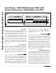
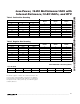
OFFSET REGISTER (00011)
FIRST BIT (MSB)
OFF15 OFF14 OFF13 OFF12 OFF11 OFF10 OFF9 OFF8
OFF7 OFF6 OFF5 OFF4 OFF3 OFF2 OFF1 OFF0
(LSB)
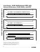
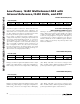
DAC2 REGISTER (00101)
Writing to the DAC1 register will update the DAC1 output
(OUT1). The output voltage in a unity gain configuration is
V
REF
x N/(2
10
), where N is the integer value of DAC1[9:0]
(0 to 1023), and V
REF
is the reference voltage for the
DAC. The DAC1 data is 10-bit long and left justified. After
power-up, the DAC1 register contains all zeros.
FIRST BIT (MSB)
DAC1[9] DAC1[8] DAC1[7] DAC1[6] DAC1[5] DAC1[4] DAC1[3] DAC1[2]
DAC1[1] DAC1[0] x xxxxx
(LSB)
DAC1 REGISTER (00100)
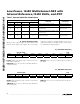
Writing to the DAC2 register will update the DAC2 output
(OUT2). The output voltage in a unity-gain configuration is
V
REF
x N/(2
10
), where N is the integer value of DAC2[9:0]
(0 to 1023), and V
REF
is the reference voltage for the
DAC. The DAC2 data is 10-bit long and left justified. After
power-up, the DAC2 register contains all zeros.
FIRST BIT (MSB)
DAC2[9] DAC2[8] DAC2[7] DAC2[6] DAC2[5] DAC2[4] DAC2[3] DAC2[2]
DAC2[1] DAC2[0] x xxxxx
(LSB)