
Datasheet


MAX1407/MAX1408/MAX1409/MAX1414
Low-Power, 16-Bit Multichannel DAS with
Internal Reference,10-Bit DACs, and RTC
______________________________________________________________________________________ 23
clocks DOUT out of the shift register. DIN and DOUT are
transferred as MSB first (data is left justified). Figure 10
shows detailed serial interface timing.
All communication with the MAX1407/MAX1408/
MAX1409/MAX1414 begins with a command byte on
DIN, where the first logic 1 on DIN will be recognized as
the START bit (MSB) for the command byte (Table 3).
The following seven clock cycles load the command into
a shift register. These seven bits specify which of the
registers will be accessed, whether a read or write oper-
ation will take place, and the length of the subsequent
data (0-bit, 8-bit, 16-bit, or burst mode). Idle DIN low
between writes to the MAX1407/MAX1408/MAX1409/
MAX1414. Figures 11–14 show the read and write timing
for 8- and 16-bit data. Data is updated on the last rising
edge of the SCLK in the command word. CS should not
go high between data transfers. If CS is toggled before
the end of a write or read operation, the device can
enter an incorrect mode. Clock in 72 zeros to clear this
state and re-arm the serial interface.
After loading the command byte into the shift register,
additional clocks shift out data on DOUT for a read and
shift in data on DIN for a write operation.
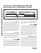
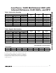
Figure 9. SPI/QSPI Interface Connections
MAX1407
MAX1408
MAX1409
MAX1414
DRDY NOT AVAILABLE ON MAX1409
RESET
CLKIN
CLKOUT
FOUT
CS
SCLK
DIN
DOUT
INT
DRDY
RESET
CLKIN
OUTPUT
SCK
MOSI
MISO
INPUT
INPUT
µP/µC
WU2 I/O
32.768kHz
WU1 I/O
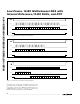
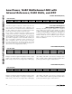
Figure 10. Detailed Serial Interface Timing
• • •
• • •
• • •
• • •
CS
SCLK
DIN
DOUT
t
CSH
t
CL
t
DS
t
DH
t
DV
t
CH
t
CYC
t
DO
t
TR
t
CSH
t
CSS