
Datasheet


MAX1407/MAX1408/MAX1409/MAX1414
Low-Power, 16-Bit Multichannel DAS with
Internal Reference,10-Bit DACs, and RTC
2 _______________________________________________________________________________________
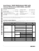
ABSOLUTE MAXIMUM RATINGS
Stresses beyond those listed under “Absolute Maximum Ratings” may cause permanent damage to the device. These are stress ratings only, and functional
operation of the device at these or any other conditions beyond those indicated in the operational sections of the specifications is not implied. Exposure to
absolute maximum rating conditions for extended periods may affect device reliability.
AV
DD
to AGND .........................................................-0.3V to +6V
AV
DD
to DV
DD
...................................................... -0.3V to +0.3V
Analog Inputs to AGND .........................-0.3V to +(AV
DD
+ 0.3V)
Digital Inputs to DGND.............................................-0.3V to +6V
Maximum Current Input Into Any Pin ..................................50mA
Continuous Power Dissipation (T
A
= +70°C)
20-Pin SSOP (derate 8.0mW/°C above +70°C) ...........640mW
28-Pin SSOP (derate 9.52mW/°C above +70°C) .........762mW
DV
DD
to DGND.........................................................-0.3V to +6V
AGND to DGND.....................................................-0.3V to +0.3V
Analog Outputs to AGND ......................-0.3V to +(AV
DD
+ 0.3V)
Digital Outputs to DGND .......................-0.3V to +(AV
DD
+ 0.3V)
REF to AGND.........................................-0.3V to +(AV
DD
+ 0.3V)
Operating Temperature Range:
MAX14__CA_ ......................................................0°C to +70°C
MAX14__EA_ ...................................................-40°C to +85°C
Lead Temperature (soldering, 10s) ................................+300 °C
Storage Temperature Range .............................-65°C to +150°C
Junction Temperature......................................................+150°C
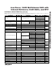
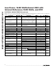
ELECTRICAL CHARACTERISTICS
(DV
DD
= AV
DD
= +2.7V to 3.6V, 4.7µF at REF, internal V
REF
, 18nF between CPLL and AV
DD
, 32.768kHz crystal across CLKIN and
CLKOUT, T
A
= T
MIN
to T
MAX
, unless otherwise noted. Typical values are at T
A
= +25°C.)
PARAMETER SYMBOL CONDITIONS MIN TYP MAX U N I T S
ADC ACCURACY
Resolution (No Missing Codes) RES 16 Bits
Unbuffered mode, Unipolar mode, gain = 1,
V
NEG
= 0.2V, fully differential input (Note 7)
1.5 3.5
U nb uffer ed m od e, U ni p ol ar m od e, g ai n = 2,
V
N E G
= 0.625V , p seud o- d i ffer enti al i np ut
1.75
Unbuffered mode, Bipolar mode, gain = 1,
V
NEG
= 0.625V, fully differential input
1.70
Integral Nonlinearity INL
Buffered mode, Bipolar mode, gain = 2,
V
NEG
= 0.625V, fully differential input
2.50
LSB
Gain = 2 ±5
Gain = 1 ±10
Unipolar
Gain = 1/3 ±30
Gain = 2 ±8
Gain = 1 ±16.5
Output RMS Noise (Note 1)
Bipolar Mode
Gain = 1/3 ±48.5
µV
RMS
Offset Error On-chip calibration removes this error ±1 % of FS R
Offset Drift ±0.5 µV/°C
Gain Error Excludes offset and reference errors ±1 % of FS R
Gain Drift Excludes offset and reference errors ±1 p p m /° C