
Datasheet


MAX1407/MAX1408/MAX1409/MAX1414
Low-Power, 16-Bit Multichannel DAS with
Internal Reference,10-Bit DACs, and RTC
14 ______________________________________________________________________________________
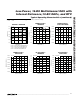
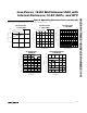
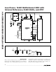
MAX1407
MAX1414
MAX1408 MAX1409 PIN FUNCTION
1 ——FB2 Force/Sense DAC2 Feedback Input
— 1 — IN7 Analog Input. Analog input to the negative mux only.
—— 1 FB1 Force/Sense DAC1 Feedback Input
22— D0 Digital Output. Three-state general-purpose digital output.
3 ——FB1 Force/Sense DAC1 Feedback Input
— 3 — IN6 Analog Input. Analog input to the negative mux only.
4 — 2 OUT1 Force/Sense DAC1 Output
— 4 — IN4 Analog Input. Analog input to the positive mux only.
5 5 3 IN0 Analog Input. Analog input to both the positive and negative mux.
6 6 4 REF
1.25V Reference Buffer Output/External Reference Input. Reference voltage
for the ADC and the DAC. Connect a 4.7µF capacitor to REF between REF
and AGND.
7 7 5 AGND
Analog Ground. Reference point for the analog circuitry. AGND connects to
the IC substrate.
886AV
DD
Analog Supply Voltage
9 9 7 CPLL
PLL Capacitor Connection Pin. Connect an 18nF ceramic capacitor between
CPLL and AV
DD
.
10 10 8 WU1
Active-Low Wake-Up Input. Internally pulled up. The device will wake-up from
Sleep mode to Standby mode when WU1 is asserted.
11 11 9 WU2
Active-Low Wake-Up Input. Internally pulled up. The device will wake-up from
Sleep mode to Standby mode when WU2 is asserted.
12 12 10 RESET
Active-Low RESET Output. It remains low while AV
DD
is below the threshold
and stays low for a timeout period after AV
DD
rises above the threshold.
RESET is an open-drain output.
13 13 — IN1 Analog Input. Analog input to both the positive and negative mux.
14 14 — IN2 Analog Input. Analog input to both the positive and negative mux.
15 15 — SHDN Programmable Shutdown Output. Goes low in Sleep mode.
16 16 — DRDY
Active-Low Data Ready Output. A logic low indicates that a new conversion
result is available in the Data register. DRDY returns high upon completion of
a full output word read operation. DRDY also signals the end of an ADC
offset-calibration.
17 17 11 FOUT 2.4576MHz Clock Output. FOUT can be used to drive the input clock of a µP.
18 18 12 CLKOUT
32kHz Crystal Output. Connect a 32kHz crystal between CLKIN and
CLKOUT.
19 19 13 CLKIN 32kHz Crystal Input. Connect a 32kHz crystal between CLKIN and CLKOUT.
Pin Description