
Datasheet


MAX13410E–MAX13415E
RS-485 Transceiver with Integrated Low-Dropout
Regulator and AutoDirection Control
2 _______________________________________________________________________________________
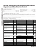
ABSOLUTE MAXIMUM RATINGS
Stresses beyond those listed under “Absolute Maximum Ratings” may cause permanent damage to the device. These are stress ratings only, and functional
operation of the device at these or any other conditions beyond those indicated in the operational sections of the specifications is not implied. Exposure to
absolute maximum rating conditions for extended periods may affect device reliability.
(All voltages referenced to GND.)
V
CC
.........................................................................-0.3V to +30V
RE, DE/RE, DE, DI, RO, V
REG
..................................-0.3V to +6V
A, B............................................................................-8V to +13V
Short-Circuit Duration (RO, A, B) to GND ................. Continuous
Continuous Power Dissipation (T
A
= +70°C)
8-Pin SO-EP (derate 19.2mW/°C above +70°C) ........1539mW
Operating Temperature Range ...........................-40°C to +85°C
Storage Temperature Range ............................-65°C to +150°C
Junction Temperature......................................................+150°C
θ
JA
(Note 1)...................................................................52.0°C/W
θ
JC
(Note 1).....................................................................6.0°C/W
Lead Temperature (soldering, 10s) ................................+300°C
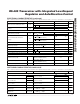
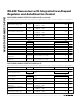
PARAMETER SYMBOL CONDITIONS MIN TYP MAX UNITS
Supply Voltage V
CC
(Note 3) 6.0 28.0 V
V
CC
= +7.5V, I
LOAD
= 20mA 4.5 5 5.5
LDO Output Voltage V
REG
V
CC
= +28V, I
LOAD
= 0mA 4.5 5 5.5
V
LDO Output Current I
REG
V
CC
> +7.5V 20
mA
LDO Dropout Voltage V
DO
V
CC
= +5V, I
OUT
= 20mA 0.5 V
Minimum Bypass Capacitor on V
REG
C
S
Guaranteed by design,
MAX13412E–MAX13415E
1µF
RE, DE = high/no load
(MAX13410E/MAX13411E)
10
Supply Current I
CC
RE, DE/RE = high, DI = low/no load
(MAX13412E–MAX13415E)
10
mA
Shutdown Current I
SHDN
DE = low, RE = high
(MAX13410E/MAX13411E)
45 µA
Thermal-Shutdown Threshold T
TS
+150 °C
Thermal-Shutdown Threshold
Hysteresis
T
TSH
15 °C
DRIVER
R
DIFF
= 100Ω, Figure 1 2.0 5.5
R
DIFF
= 54Ω, Figure 1 1.5 5.5Differential Driver Output V
OD
No load 5.5
V
Change in Magnitude of Differential
Output Voltage
ΔV
OD
R
DIFF
= 100Ω or 54Ω, Figure 1 0.2 V
Driver Common-Mode Output Voltage V
OC
R
DIFF
= 100Ω or 54Ω, Figure 1 1 3 V
Change In Magnitude of Common-
Mode Voltage
ΔV
OC
R
DIFF
= 100Ω or 54Ω, Figure 1 0.2 V
Input High Voltage V
IH
DI, DE, RE, DE/RE 2.0 V
Input Low Voltage V
IL
DI, DE, RE, DE/RE 0.8 V
Input Current I
IN
DI, DE, RE, DE/RE ±1 µA
Driver-Disable Threshold V
DT
T
A
= +25°C (MAX13412E/MAX13413E) 0.6 1.0 V
Note 1: Package thermal resistances were obtained using the method described in JEDEC specificactions JESD51-7 using a four layer board.
For detailed information on package consitencies refer to www.maxim-ic/thermal-tutorial.
ELECTRICAL CHARACTERISTICS
(V
CC
= +6.0V to +28V, T
A
= T
MIN
to T
MAX
, unless otherwise noted. Typical values are at V
CC
= +7.5V, C
S
= 1µF, and T
A
= +25°C.) (Note 2)