
Datasheet


MAX1303
Track-and-Hold Circuitry
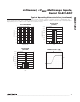
The MAX1303 features a switched-capacitor T/H archi-
tecture that allows the analog input signal to be stored as
charge on sampling capacitors. See Figures 1, 2, and 3
for T/H timing and the sampling instants for each operat-
ing mode. The MAX1303 analog input circuitry buffers
the input signal from the sampling capacitors, resulting
in a constant analog input impedance with varying input
voltage (Figure 4).
Analog Input Circuitry
Select differential or single-ended conversions using the
associated analog input configuration byte (Table 2).
The analog input signal source must be capable of dri-
ving the ADC’s 6kΩ input resistance (Figure 5).
Figure 5 shows the simplified analog input circuit. The
analog inputs are ±6V fault tolerant and are protected
by back-to-back diodes. The summing junction voltage,
V
SJ
, is a function of the channel’s input common-mode
voltage:
As a result, the analog input impedance is relatively
constant over the input voltage as shown in Figure 4.
Single-ended conversions are internally referenced to
AGND1 (Tables 3 and 4). In differential mode, IN+ and
IN- are selected according to Tables 3 and 5. When con-
figuring differential channels, the differential pair follows
the analog configuration byte for the positive channel.
For example, to configure CH2 and CH3 for a ±V
REF
dif-
ferential conversion, set the CH2 analog configuration
byte for a differential conversion with the ±V
REF
range
(1010 1100). To initiate a conversion for the CH2 and
CH3 differential pair, issue the command 1010 0000.
V
R
RR
V
R
RR
V
SJ CM
.
=
+
⎛
⎝
⎜
⎞
⎠
⎟
×++
+
⎛
⎝
⎜
⎞
⎠
⎟
⎛
⎝
⎜
⎞
⎠
⎟
×
1
12
2 375 1
1
12
4-Channel, ±V
REF
Multirange Inputs,
Serial 16-Bit ADC
14 ______________________________________________________________________________________
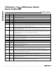
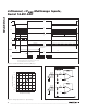
CS
SCLK
1
2
3
4
5
6
7
8
9
10
11
12
13
14
15
16
17
18
19
20
21
22
23
24
25
26
27
28
29
30
31
32
DIN S C2 C1 C0 0 0 0 0
ANALOG INPUT
TRACK AND HOLD*
DOUT
B15 B14 B13 B12 B11 B10 B9 B8 B7 B6 B5 B4 B3 B2 B1 B0
BYTE 1 BYTE 2 BYTE 3 BYTE 4
SSTRB
HOLD TRACK HOLD
HIGH
IMPEDANCE
t
ACQ
HIGH
IMPEDANCE
*TRACK AND HOLD TIMING IS CONTROLLED BY SCLK.
f
SAMPLE
≈ f
SCLK
/32
SAMPLING INSTANT
Figure 1. External Clock-Mode Conversion (Mode 0)