
Datasheet


MAX1295/MAX1297
265ksps, +3V, 6-/2-Channel, 12-Bit ADCs
with +2.5V Reference and Parallel Interface
______________________________________________________________________________________ 15
Shutdown Mode
Shutdown mode turns off all chip functions that draw qui-
escent current, reducing the typical supply current to
2µA immediately after the current conversion is complet-
ed. A rising edge on WR causes the MAX1295/MAX1297
to exit shutdown mode and return to normal operation.
To achieve full 12-bit accuracy with a 4.7µF reference
bypass capacitor, 50µs is required after power-up.
Waiting 50µs in standby mode, instead of in full-power
mode, can reduce power consumption by a factor of 3 or
more. When using an external reference, only 50µs is
required after power-up. Enter standby mode by per-
forming a dummy conversion with the control byte speci-
fying standby mode.
Note: Bypass capacitors larger than 4.7µF between
REF and GND result in longer power-up delays.
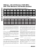
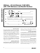
Transfer Function
Table 5 shows the full-scale voltage ranges for unipolar
and bipolar modes. Figure 8 depicts the nominal unipo-
lar input/output (I/O) transfer function, and Figure 9
shows the bipolar I/O transfer function. Code transitions
occur halfway between successive-integer LSB values.
Output coding is binary, with 1 LSB = (V
REF
/ 4096).
Maximum Sampling Rate/
Achieving 300ksps
When running at the maximum clock frequency of
4.8MHz, the specified throughput of 265ksps is achieved
by completing a conversion every 18 clock cycles: 1
write cycle, 3 acquisition cycles, 13 conversion cycles,
and 1 read cycle. This assumes that the results of the
last conversion are read before the next control byte is
written. It is possible to achieve higher throughputs, up
to 300ksps, by first writing a control byte to begin the
Table 5. Full-Scale and Zero-Scale for Unipolar and Bipolar Operation
111 . . . 111
111 . . . 110
100 . . . 010
100 . . . 001
100 . . . 000
011 . . . 111
011 . . . 110
011 . . . 101
000 . . . 001
000 . . . 000
1
0
INPUT VOLTAGE (LSB)
OUTPUT CODE
ZS = COM
FS = REF + COM
1 LSB =
REF
4096
FULL-SCALE
TRANSITION
(COM)
FS - 3/2 LSB
FS
2
2048
UNIPOLAR MODE BIPOLAR MODE
COM COMZero ScaleZero Scale
V
REF
+ COM
V
REF
/2 + COMPositive Full Scale
Full Scale
-V
REF
/2 + COM Negative Full Scale
Figure 8. Unipolar Transfer Function
011 . . . 111
011 . . . 110
000 . . . 010
000 . . . 001
000 . . . 000
111 . . . 111
111 . . . 110
111 . . . 101
100 . . . 001
100 . . . 000
- FS
COM*
INPUT VOLTAGE (LSB)
OUTPUT CODE
ZS = COM
+FS - 1 LSB
*COM ≥ V
REF
/2
+ COM
FS
=
REF
2
-FS = + COM
-REF
2
1 LSB =
REF
4096
Figure 9. Bipolar Transfer Function