
Datasheet


MAX1294/MAX1296
420ksps, +5V, 6-/2-Channel, 12-Bit ADCs
with +2.5V Reference and Parallel Interface
_______________________________________________________________________________________ 9
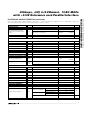
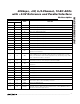
BIT
PD1, PD0
0
D7, D6
PD1 and PD0 select the various clock and power-down modes.
Full Power-Down Mode. Clock mode is unaffected.
D5 ACQMOD
ACQMOD = 0: Internal Acquisition Mode
ACQMOD = 1: External Acquisition Mode
NAME FUNCTIONAL DESCRIPTION
0
10
Standby Power-Down Mode. Clock mode is unaffected.
0
11
Normal Operation Mode. External clock mode selected.
1
Normal Operation Mode. Internal clock mode selected.
D4
SGL/DIF
SGL/DIF = 0: Pseudo-Differential Analog Input Mode
SGL/DIF = 1: Single-Ended Analog Input Mode
In single-ended mode, input signals are referred to COM. In pseudo-differential mode, the voltage
difference between two channels is measured (see Tables 2, 4).
D3
UNI/BIP
UNI/BIP = 0: Bipolar Mode
UNI/BIP = 1: Unipolar Mode
In unipolar mode, an analog input signal from 0V to V
REF
can be converted; in bipolar mode, the
signal can range from -V
REF
/2 to +V
REF
/2.
D2, D1, D0 A2, A1, A0
Address bits A2, A1, A0 select which of the 6/2 (MAX1294/MAX1296) channels is to be converted
(see Tables 2, 3).
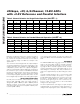
Table 1. Control-Byte Functional Description
Single-Ended and
Pseudo-Differential Operation
The sampling architecture of the ADCs’ analog com-
parator is illustrated in the equivalent input circuits of
Figure 3. In single-ended mode, IN+ is internally
switched to channels CH0–CH5 for the MAX1294
(Figure 3a) and to CH0–CH1 for the MAX1296 (Figure
3b), while IN- is switched to COM (Table 2). In differen-
tial mode, IN+ and IN- are selected from analog input
pairs (Table 3) and are internally switched to either of
the analog inputs. This configuration is pseudo-differen-
tial to the effect that only the signal at IN+ is sampled.
The return side (IN-) must remain stable within ±0.5
LSB (±0.1 LSB for best performance) with respect to
GND during a conversion. To accomplish this, connect
a 0.1µF capacitor from IN- (the selected input) to GND.
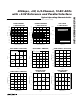
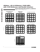
Figure 3a. MAX1294 Simplified Input Structure Figure 3b. MAX1296 Simplified Input Structure
CH0
CH1
CH3
CH2
CH5
CH4
COM
C
SWITCH
TRACK
T/H
SWITCH
R
IN
800Ω
C
HOLD
HOLD
12-BIT CAPACITIVE DAC
V
REF
ZERO
COMPARATOR
–
+
12pF
SINGLE-ENDED MODE: IN+ = CH0–CH5, IN- = COM.
DIFFERENTIAL MODE: IN+ AND IN- SELECTED FROM PAIRS OF
CH0/CH1 AND CH2/CH3, AND CH4/CH5
AT THE SAMPLING INSTANT,
THE MUX INPUT SWITCHES
FROM THE SELECTED IN+
CHANNEL TO THE SELECTED
IN- CHANNEL.
INPUT
MUX
CH0
CH1
COM
C
SWITCH
TRACK
T/H
SWITCH
R
IN
800Ω
C
HOLD
HOLD
12-BIT CAPACITIVE DAC
V
REF
ZERO
COMPARATOR
–
+
12pF
SINGLE-ENDED MODE: IN+ = CH0–CH1, IN- = COM.
DIFFERENTIAL MODE: IN+ AND IN- SELECTED FROM PAIR
CH0/CH1.
AT THE SAMPLING INSTANT,
THE MUX INPUT SWITCHES
FROM THE SELECTED IN+
CHANNEL TO THE SELECTED
IN- CHANNEL.
INPUT
MUX