
Datasheet


MAX1294/MAX1296
420ksps, +5V, 6-/2-Channel, 12-Bit ADCs
with +2.5V Reference and Parallel Interface
8 _______________________________________________________________________________________
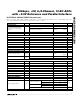
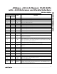
Pin Description (continued)
PIN
MAX1296
REF
2125
MAX1294
NAME
Bandgap Reference Buffer Output/External Reference Input. Add a 4.7µF capacitor
to GND when using the internal reference.
FUNCTION
26 22 V
DD
Analog +5V Power Supply. Bypass with a 0.1µF capacitor to GND.
27 23 D11 Three-State Digital Output (D11)
28 24 D10 Three-State Digital Output (D10)
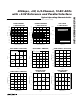
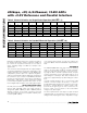
_______________Detailed Description
Converter Operation
The MAX1294/MAX1296 ADCs use a successive-approx-
imation (SAR) conversion technique and an input
track/hold (T/H) stage to convert an analog input signal to
a 12-bit digital output. This output format provides easy
interface to standard microprocessors (µPs). Figure 2
shows the simplified internal architecture of the MAX1294/
MAX1296.
T/H
THREE-STATE, BIDIRECTIONAL
I/O INTERFACE
12
17kΩ
12
SUCCESSIVE-
APPROXIMATION
REGISTER
CHARGE REDISTRIBUTION
12-BIT DAC
CLOCK
ANALOG
INPUT
MULTIPLEXER
CONTROL LOGIC
&
LATCHES
REF REFADJ
1.22V
REFERENCE
D0–D11
12-BIT DATA BUS
(CH5)
(CH4)
(CH3)
(CH2)
CH1
CH0
COM
CLK
CS
( ) ARE FOR MAX1294 ONLY.
WR
RD
INT
V
DD
GND
MAX1294
MAX1296
A
V
=
2.05
COMP
Figure 2. Simplified Functional Diagram