
Datasheet


MAX1294/MAX1296
420ksps, +5V, 6-/2-Channel, 12-Bit ADCs
with +2.5V Reference and Parallel Interface
______________________________________________________________________________________ 13
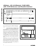
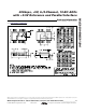
External Clock Mode
To select external clock mode, bits D6 and D7 of the
control byte must be set to 1. Figure 6 shows the clock
and WR timing relationship for internal (Figure 6a) and
external (Figure 6b) acquisition modes with an external
clock. For proper operation, a 100kHz to 7.6MHz clock
frequency with 30% to 70% duty cycle is recommended.
Operating the MAX1294/MAX1296 with clock frequen-
cies lower than 100kHz is not recommended because
the resulting voltage droop across the hold capacitor in
the T/H stage degrades performance.
Digital Interface
The input and output data are multiplexed on a three-
state parallel interface (I/O) that can easily be inter-
faced with standard µPs. The signals CS, WR, and RD
control the write and read operations. CS represents
the chip-select signal, which enables a µP to address
the MAX1294/MAX1296 as an I/O port. When high, CS
disables the CLK, WR, and RD inputs and forces the
interface into a high-impedance (high-Z) state.
Figure 6a. External Clock and
WR
Timing (Internal Acquisition Mode)
Figure 6b. External Clock and
WR
Timing (External Acquisition Mode)
WR
CLK
CLK
WR
WR GOES HIGH WHEN CLK IS HIGH
WR GOES HIGH WHEN CLK IS LOW
t
CWS
t
CH
t
CL
t
CP
t
CWH
ACQUISITION STARTS
ACQUISITION STARTS
CONVERSION STARTS
CONVERSION STARTS
ACQUISITION ENDS
ACQUISITION ENDS
ACQMOD = "0"
ACQMOD = "0"
WR
CLK
CLK
WR
WR GOES HIGH WHEN CLK IS HIGH
WR GOES HIGH WHEN CLK IS LOW
t
DH
t
DH
t
CWH
t
CWS
ACQUISITION STARTS
ACQUISITION STARTS
CONVERSION STARTS
CONVERSION STARTS
ACQUISITION ENDS
ACQUISITION ENDS
ACQMOD = "1"
ACQMOD = "1"
ACQMOD = "0"
ACQMOD = "0"