
Datasheet


MAX1294/MAX1296
420ksps, +5V, 6-/2-Channel, 12-Bit ADCs
with +2.5V Reference and Parallel Interface
10 ______________________________________________________________________________________
During the acquisition interval, the channel selected as
the positive input (IN+) charges capacitor C
HOLD
. At
the end of the acquisition interval, the T/H switch
opens, retaining charge on C
HOLD
as a sample of the
signal at IN+.
The conversion interval begins with the input multiplex-
er switching C
HOLD
from the positive input (IN+) to the
negative input (IN-). This unbalances node ZERO at the
comparator’s positive input. The capacitive digital-to-
analog converter (DAC) adjusts during the remainder of
the conversion cycle to restore node ZERO to 0V within
the limits of 12-bit resolution. This action is equivalent to
transferring a 12pF [(V
IN
+ - V
IN
-)] charge from C
HOLD
to the binary-weighted capacitive DAC, which in turn
forms a digital representation of the analog input signal.
Analog Input Protection
Internal protection diodes, which clamp the analog
input to V
DD
and GND, allow each input channel to
swing within (GND - 300mV) to (V
DD
+ 300mV) without
damage. However, for accurate conversions near full
scale, both inputs must not exceed (V
DD
+ 50mV) or be
less than (GND - 50mV).
If an analog input voltage exceeds the supplies by
more than 50mV, limit the forward-bias input current to
4mA.
Track/Hold
The MAX1294/MAX1296 T/H stage enters its tracking
mode on the rising edge of WR. In external acquisition
mode, the part enters its hold mode on the next on ris-
ing edge of WR. In internal acquisition mode, the part
enters its hold mode on the fourth falling edge of clock
after writing the control byte. Note that, in internal clock
mode, this is approximately 1µs after writing the control
byte.
In single-ended operation, IN- is connected to COM
and the converter samples the positive “+” input. In
pseudo-differential operation, IN- connects to the nega-
tive input “-”, and the difference of
|
(IN+) - (IN-)
|
is sam-
pled. At the beginning of the next conversion, the
positive input connects back to IN+ and C
HOLD
charges to the input signal.
The time required for the T/H stage to acquire an input
signal depends on how quickly its input capacitance is
charged. If the input signal’s source impedance is high,
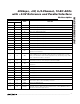
A1 CH0
0 +00
A0
0 1
CH2* CH4*
+0
1 0 +
CH3*
0
CH1
1
CH5*
1 +0
0 0
A2
+1
0 1 +1
Table 2. Channel Selection for Single-Ended Operation (SGL/DIF = 1)
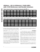
Table 3. Channel Selection for Pseudo-Differential Operation (SGL/DIF = 0)
A1 CH0
0 +00
A0
0 1
CH2* CH4*
+0
1 0 + -
CH3*
0
CH1
1
CH5*
1 +0
0 0
A2
+ -1
0 1 - +1
*Channels CH2–CH5 apply to MAX1294 only.
*Channels CH2–CH5 apply to MAX1294 only.
-
-
-
COM
-
-
-