
Datasheet


Note 1: Accuracy specifications tested at V
DD
= 5.0V. Performance at power-supply tolerance limits is guaranteed by Power-Supply
Rejection test.
Note 2: External reference: V
REF
= 4.096V, offset error nulled, ideal last-code transition = FS - 3/2 LSB.
Note 3: Ground “on” channel, sine wave applied to all “off” channels.
Note 4: Guaranteed by design. Not tested.
Note 5: Use static external load during conversion for specified accuracy.
Note 6: Tested using internal reference.
Note 7: PSRR measured at full scale. Tested for the ±10V (MAX127) and ±4.096V (MAX128) input ranges.
Note 8: Not subject to production testing. Provided for design guidance only.
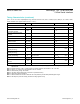
(V
DD
= +4.75V to +5.25V; unipolar/bipolar range; external reference mode, V
REF
= 4.096V; 4.7μF at REF pin; T
A
= T
MIN
to T
MAX
,
unless otherwise noted. Typical values are at T
A
= +25°C.)
PARAMETER SYMBOL CONDITIONS MIN TYP MAX UNITS
2-WIRE STANDARD MODE
SCL Clock Frequency f
SCL
100 kHz
Bus Free Time Between a STOP
and START Condition
t
BUF
4.7 µs
Hold Time (Repeated) START
Condition
t
HD,STA
4.0 µs
Low Period of the SCL Clock t
LOW
4.7 µs
High Period of the SCL Clock t
HIGH
4.0 µs
Setup Time for a Repeated
START Condition
t
SU, STA
4.7 µs
Data Hold Time t
HD, DAT
0 0.9 µs
Data Setup Time t
SU, DAT
250 ns
Rise Time for Both SDA and SCL
Signals (Receiving)
t
R
1000 ns
Fall Time for Both SDA and SCL
Signals (Receiving)
t
F
300 ns
Fall Time for Both SDA and SCL
Signals (Transmitting)
t
F
C
b
= total capacitance of one bus line in pF,
up to 6mA sink
20 +
0.1 x C
b
250 ns
Setup Time for STOP Condition t
SU, STO
4.0 µs
Capacitive Load for Each
Bus Line
C
b
400 pF
Pulse Width of Spike Suppressed t
SP
0 50 ns
MAX127/MAX128 Multirange, +5V, 12-Bit DAS with
2-Wire Serial Interface
www.maximintegrated.com
Maxim Integrated
│
6
Timing Characteristics (continued)