
Datasheet


Supply Current
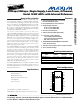
MAX1280/MAX1281
400ksps/300ksps, Single-Supply, Low-Power, 8-Channel,
Serial 12-Bit ADCs with Internal Reference
4 _______________________________________________________________________________________
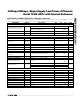
CONDITIONS
mA
2.5 4.0
I
VDD1 +
I
VDD2
Supply Current
V4.5 5.5
V
DD1
,
V
DD2
Positive Supply Voltage
(Note 9)
1.3 2.0
0.9 1.5
µA210
UNITSMIN TYP MAXSYMBOLPARAMETER
V
DD1
=
V
DD2
= 5.5V
ELECTRICAL CHARACTERISTICS—MAX1281
(V
DD1
= V
DD2
= +2.7V to +3.6V, COM = GND, f
SCLK
= 4.8MHz, 50% duty cycle, 16 clocks/conversion cycle (300ksps), external
+2.5V at REF, REFADJ = V
DD1
, T
A
= T
MIN
to T
MAX
, unless otherwise noted. Typical values are at T
A
= +25°C.)
SINAD > 68dB
-3dB point
f
IN
= 150kHz, V
IN
= 2.5Vp-p
f
IN1
= 73kHz, f
IN2
= 77kHz
No missing codes over temperature
Up to the 5th harmonic
CONDITIONS
kHz
250
Full-Linear Bandwidth
MHz
3
Full-Power Bandwidth
dB
-78
Channel-to-Channel Crosstalk
(Note 4)
dB
76
IMDIntermodulation Distortion
dB
80
SFDR
Spurious-Free Dynamic
Range
dB
-81
THDTotal Harmonic Distortion
LSB
±1.0
INLRelative Accuracy (Note 2)
Bits
12
Resolution
dB
70
SINAD
Signal-to-Noise plus
Distortion Ratio
LSB
±0.2
Channel-to-Channel Offset-
Error Matching
ppm/°C
±1.6
Gain-Error Temperature
Coefficient
LSB
±1.0
DNLDifferential Nonlinearity
LSB
±6.0
Offset Error
LSB
±7.0
Gain Error (Note 3)
UNITSMIN TYP MAXSYMBOLPARAMETER
Operating mode (Note 10)
Reduced-power mode (Note 11)
Fast power-down (Note 11)
Full power-down (Note 11)
V
DD1
= V
DD2
= 5V ±10%, midscale input mV±0.5 ±2.0PSRPower-Supply Rejection
POWER SUPPLY
DC ACCURACY (Note 1)
DYNAMIC SPECIFICATIONS (75kHz sine-wave input, 2.5Vp-p, 300ksps, 4.8MHz clock, bipolar input mode)
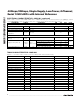
ELECTRICAL CHARACTERISTICS—MAX1280 (continued)
(V
DD1
= V
DD2
= +4.5V to +5.5V, COM = GND, f
SCLK
= 6.4MHz, 50% duty cycle, 16 clocks/conversion cycle (400ksps), external
+2.5V at REF, REFADJ = V
DD1
, T
A
= T
MIN
to T
MAX
, unless otherwise noted. Typical values are at T
A
= +25°C.)