
Datasheet


MAX1280/MAX1281
400ksps/300ksps, Single-Supply, Low-Power, 8-Channel,
Serial 12-Bit ADCs with Internal Reference
12 ______________________________________________________________________________________
10µF0.1µF
2.5V
V
DD1
V
DD2
GND
COM
CS
SCLK
DIN
DOUT
SSTRB
SHDN
TO V
DD2
TO V
DD2
0.01µF
CH7
REFADJ
REF
4.7µF
0V TO
2.500V
ANALOG
INPUT
OSCILLOSCOPE
CH1 CH2
CH3 CH4
*FULL-SCALE ANALOG INPUT, CONVERSION RESULT = $FFF (HEX)
MAX1280
MAX1281
+3V or +5V
EXTERNAL CLOCK
SCLK
SSTRB
DOUT*
0.01µF
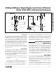
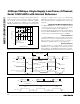
Figure 5. Quick-Look Circuit
Track/Hold
The T/H enters its tracking mode on the falling clock
edge after the fifth bit of the 8-bit control word has been
shifted in. It enters its hold mode on the falling clock
edge after the eighth bit of the control word has been
shifted in. If the converter is set up for single-ended
inputs, IN- is connected to COM and the converter con-
verts the “+” input. If the converter is set up for differen-
tial inputs, the difference of [(IN+) - (IN-)] is converted.
At the end of the conversion, the positive input con-
nects back to IN+ and C
HOLD
charges to the input sig-
nal.
The time required for the T/H to acquire an input signal
is a function of how quickly its input capacitance is
charged. If the input signal’s source impedance is high,
the acquisition time lengthens, and more time must be
allowed between conversions. The acquisition time,
t
ACQ
, is the maximum time the device takes to acquire
the signal and is also the minimum time needed for the
signal to be acquired. It is calculated by the following
equation:
t
ACQ
= 9
✕
(R
S
+ R
IN
)
✕
12pF
where R
IN
= 800Ω, R
S
= the source impedance of the
input signal; t
ACQ
is never less than 468ns (MAX1280)
or 625ns (MAX1281). Note that source impedances
below 2kΩ do not significantly affect the ADC’s AC per-
formance.
Input Bandwidth
The ADC’s input tracking circuitry has a 6MHz
(MAX1280) or 3MHz (MAX1281) small-signal band-
width, so it is possible to digitize high-speed transient
events and measure periodic signals with bandwidths
exceeding the ADC’s sampling rate by using under-
sampling techniques. To avoid high-frequency signals
being aliased into the frequency band of interest, anti-
alias filtering is recommended.
Analog Input Protection
Internal protection diodes, which clamp the analog
input to V
DD1
and GND, allow the channel input pins to
swing from GND - 0.3V to V
DD1
+ 0.3V without dam-
age. However, for accurate conversions near full scale,
the inputs must not exceed V
DD1
by more than 50mV or
be lower than GND by 50mV.
If the analog input exceeds 50mV beyond the sup-
plies, do not allow the input current to exceed 2mA.
Quick Look
To quickly evaluate the MAX1280/MAX1281’s analog
performance, use the circuit of Figure 5. The MAX1280/
MAX1281 require a control byte to be written to DIN
before each conversion. Connecting DIN to V
DD2
feeds
in control bytes of $FF (HEX), which trigger single-
ended unipolar conversions on CH7 without powering
down between conversions. The SSTRB output pulses