
Datasheet


MAX1280/MAX1281
400ksps/300ksps, Single-Supply, Low-Power, 8-Channel,
Serial 12-Bit ADCs with Internal Reference
______________________________________________________________________________________ 11
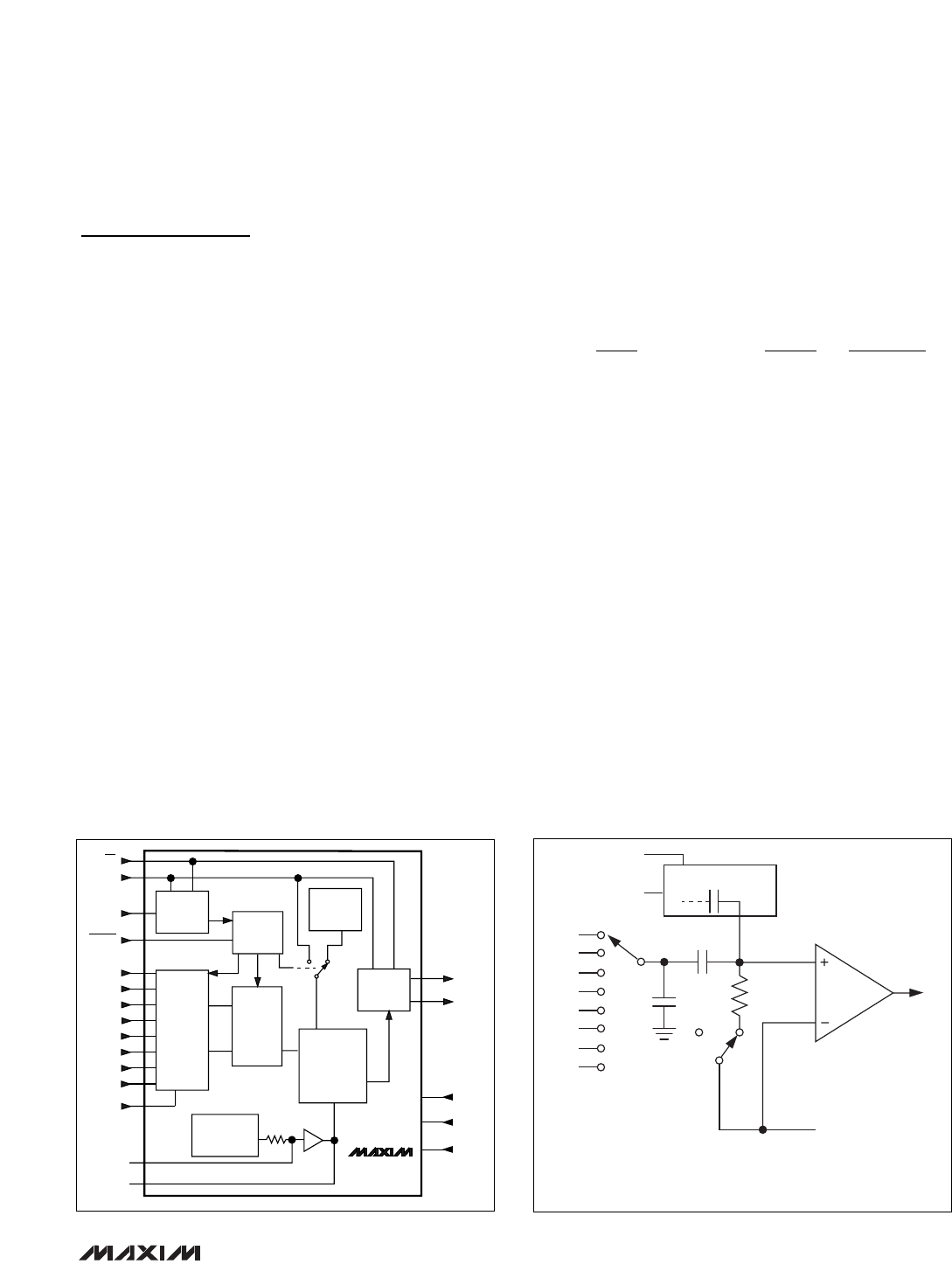
Detailed Description
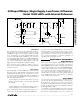
The MAX1280/MAX1281 analog-to-digital converters
(ADCs) use a successive-approximation conversion tech-
nique and input track/hold (T/H) circuitry to convert an
analog signal to a 12-bit digital output. A flexible serial
interface provides easy interface to microprocessors
(µPs). Figure 3 shows a functional diagram of the
MAX1280/MAX1281.
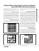
Pseudo-Differential Input
The equivalent input circuit of Figure 4 shows the
MAX1280/MAX1281’s input architecture, which is com-
posed of a T/H, input multiplexer, input comparator,
switched-capacitor DAC, and reference.
In single-ended mode, the positive input (IN+) is con-
nected to the selected input channel and the negative
input (IN-) is set to COM. In differential mode, IN+ and
IN- are selected from the following pairs: CH0/CH1,
CH2/CH3, CH4/CH5, and CH6/CH7. Configure the
channels according to Tables 2 and 3.
The MAX1280/MAX1281 input configuration is pseudo-
differential in that only the signal at IN+ is sampled. The
return side (IN-) is connected to the sampling capacitor
while converting and must remain stable within ±0.5LSB
(±0.1LSB for best results) with respect to GND during a
conversion.
If a varying signal is applied to the selected IN-, its ampli-
tude and frequency must be limited to maintain accuracy.
The following equations determine the relationship
between the maximum signal amplitude and its frequency
in order to maintain ±0.5LSB accuracy. Assuming a sinu-
soidal signal at IN-, the input voltage is determined by:
The maximum voltage variation is determined by:
A 650mVp-p 60Hz signal at IN- will generate ±0.5LSB
of error when using a +2.5V reference voltage and a
2.5µs conversion time (15/f
SCLK
). When a DC reference
voltage is used at IN-, connect a 0.1µF capacitor to
GND to minimize noise at the input.
During the acquisition interval, the channel selected as
the positive input (IN+) charges capacitor C
HOLD
. The
acquisition interval spans three SCLK cycles and ends
on the falling SCLK edge after the last bit of the input
control word has been entered. At the end of the acqui-
sition interval, the T/H switch opens, retaining charge
on C
HOLD
as a sample of the signal at IN+. The conver-
sion interval begins with the input multiplexer switching
C
HOLD
from IN+ to IN-. This unbalances node ZERO at
the comparator’s input. The capacitive DAC adjusts
during the remainder of the conversion cycle to restore
node ZERO to V
DD1
/2 within the limits of 12-bit
resolution. This action is equivalent to transferring a
12pF x (V
IN
+ - V
IN
-) charge from C
HOLD
to the binary-
weighted capacitive DAC, which in turn forms a digital
representation of the analog input signal.
max
d
-
d
-
2f
1LSB
t
V
2t
IN
t
IN
CONV
REF
12
CONV
ν
π=
()
≤ =V
νπ
IN IN--
sin(2 ft)=
()
V
INPUT
SHIFT
REGISTER
CONTROL
LOGIC
INT
CLOCK
OUTPUT
SHIFT
REGISTER
+1.22V
REFERENCE
T/H
ANALOG
INPUT
MUX
12-BIT
SAR
ADC
IN
DOUT
SSTRB
V
DD1
V
DD2
GND
SCLK
DIN
COM
REFADJ
REF
OUT
REF
CLOCK
+2.500V
17kΩ
10
9
12
11
14
15
16
17
18
CH6
7
CH7
8
CH4
5
CH5
6
CH1
2
CH2
3
CH3
4
CH0
1
MAX1280
MAX1281
CS
SHDN
20
19
13
≈ 2.05*
A
Figure 3. Functional Diagram
C
HOLD
R
IN
800Ω
12pF
HOLD
INPUT
MUX
C
SWITCH
*
*INCLUDES ALL INPUT PARASITICS
SINGLE-ENDED MODE: IN+ = CH0–CH7, IN- = COM.
PSEUDO-DIFFERENTIAL MODE: IN+ AND IN- SELECTED FROM
PAIRS OF CH0/CH1, CH2/CH3, CH4/CH5, AND CH6/CH7.
AT THE SAMPLING INSTANT,
THE MUX INPUT SWITCHES FROM
THE SELECTED IN+ CHANNEL TO
THE SELECTED IN- CHANNEL.
CH0
REF
GND
CH1
CH2
CH3
CH4
CH5
CH6
CH7
ZERO
V
DD1
/2
COMPARATOR
CAPACITATIVE
DAC
6pF
TRACK
Figure 4. Equivalent Input Circuit