
Datasheet


MAX1274/MAX1275
1.8Msps, Single-Supply, Low-Power,
True-Differential, 12-Bit ADCs
8 _______________________________________________________________________________________
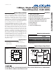
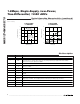
Pin Description
PIN NAME FUNCTION
1 AIN- Negative Analog Input
2 REF
External Reference Voltage Input. V
REF
sets the analog input range. Bypass REF with a 0.01µF
capacitor and a 4.7µF capacitor to RGND.
3 RGND Reference Ground. Connect RGND to GND.
4V
DD
Positive Analog Supply Voltage (+4.75V to +5.25V). Bypass V
DD
with a 0.01µF capacitor and a 10µF
capacitor to GND.
5, 11 N.C. No Connection
6 GND Ground. GND is internally connected to EP.
7V
L
Positive Logic Supply Voltage (1.8V to V
DD
). Bypass V
L
with a 0.01µF capacitor and a 10µF capacitor
to GND.
8 DOUT Serial Data Output. Data is clocked out on the rising edge of SCLK.
9 CNVST
Convert Start. Forcing CNVST high prepares the part for a conversion. Conversion begins on the
falling edge of CNVST. The sampling instant is defined by the falling edge of CNVST.
10 SCLK Serial Clock Input. Clocks data out of the serial interface. SCLK also sets the conversion speed.
12 AIN+ Positive Analog Input
— EP Exposed Paddle. EP is internally connected to GND.
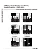
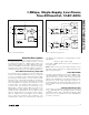
Typical Operating Characteristics (continued)
(V
DD
= +5V, V
L
= V
DD
, V
REF
= 4.096V, f
SCLK
= 28.8MHz, T
A
= -40°C to +85°C, unless otherwise noted. Typical values are measured
at T
A
= +25°C)
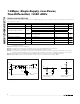
V
L
SUPPLY CURRENT
vs. TEMPERATURE
MAX1274 toc22
TEMPERATURE (°C)
V
L
SUPPLY CURRENT (mA)
603510-15
0.2
0.4
0.6
0.8
1.0
0
-40 85
CONVERTING
f
SCLK
= 28.8MHz
FULL/PARTIAL
POWER-DOWN
f
SCLK
= 28.8MHz
V
L
SUPPLY CURRENT
vs. CONVERSION RATE
MAX1274 toc23
f
SAMPLE
(kHz)
V
L
SUPPLY CURRENT (mA)
15001000500
0.3
0.5
0.8
1.0
0
0 2000
V
L
= 5V
V
L
= 3V
V
L
= 1.8V