
Datasheet
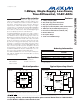


MAX1274/MAX1275
1.8Msps, Single-Supply, Low-Power,
True-Differential, 12-Bit ADCs
_______________________________________________________________________________________ 3
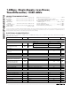
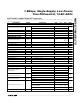
ELECTRICAL CHARACTERISTICS (continued)
(V
DD
= +5V ±5%, V
L
= V
DD
, V
REF
= 4.096V, f
SCLK
= 28.8MHz, 50% duty cycle, T
A
= -40°C to +85°C, unless otherwise noted. Typical
values are at T
A
= +25°C.)
PARAMETER SYMBOL CONDITIONS MIN TYP MAX UNITS
ANALOG INPUTS (AIN+, AIN-)
AIN+ - AIN-, MAX1274 0 V
REF
Differential Input Voltage Range V
IN
AIN+ - AIN-, MAX1275 -V
REF
/2 +V
REF
/2
V
Absolute Input Voltage Range 0 V
DD
V
DC Leakage Current ±1 µA
Input Capacitance Per input pin 16 pF
Input Current (Average) Time averaged at maximum throughput rate 75 µA
REFERENCE INPUT (REF)
REF Input Voltage Range V
REF
1.0
V
DD
+
50mV
V
Input Capacitance 20 pF
DC Leakage Current ±1 µA
Input Current (Average) Time averaged at maximum throughput rate 400 µA
DIGITAL INPUTS (SCLK, CNVST)
Input Voltage Low V
IL
0.3 x V
L
V
Input Voltage High V
IH
0.7 x V
L
V
Input Leakage Current I
IL
0.05 ±10 µA
DIGITAL OUTPUT (DOUT)
Output Load Capacitance C
OUT
For stated timing performance 30 pF
Output Voltage Low V
OL
I
SINK
= 5mA, V
L
≥ 1.8V 0.4 V
Output Voltage High V
OH
I
SOURCE
= 1mA, V
L
≥ 1.8V V
L
- 0.5V V
Output Leakage Current I
OL
Output high impedance ±0.2 ±10 µA
POWER REQUIREMENTS
Analog Supply Voltage V
DD
4.75 5.25 V
Digital Supply Voltage V
L
1.8 V
DD
V
Static, f
SCLK
= 28.8MHz 7 9
Static, no SCLK 4 5
Analog Supply Current,
Normal Mode
I
DD
Operational, 1.8Msps 9 11
mA
f
SCLK
= 28.8MHz 1
Analog Supply Current,
Partial Power-Down Mode
I
DD
No SCLK 1
mA
f
SCLK
= 28.8MHz 1
Analog Supply Current,
Full Power-Down Mode
I
DD
No SCLK 1
µA
Operational, full-scale input at 1.8Msps 1 2.5
Static, f
SCLK
= 28.8MHz 0.4 1
Partial/full power-down mode,
f
SCLK
= 28.8MHz
0.2 0.5
mA
Digital Supply Current (Note 7)
Static, no SCLK, all modes 0.1 1 µA
Positive-Supply Rejection PSR V
DD
= 5V ±5%, full-scale input ±0.2 ±3.0 mV