
Datasheet


frame sync (TXM = 1), CLKX driven by an on-chip clock
source (MCM = 1), burst mode (FSM = 1), and 16-bit
word length (FO = 0).
This setup allows continuous conversions provided that
the data transmit register (DXR) and the data-receive
register (DRR) are serviced before the next conversion.
Alternatively, autobuffering can be enabled when using
the buffered serial port to execute conversions and
read the data without CPU intervention. Connect the V
L
pin to the TMS320C54_ supply voltage when the
MAX1274/MAX1275 are operating with an analog sup-
ply voltage higher than the DSP supply voltage. The
word length can be set to 8 bits with FO = 1 to imple-
ment the power-down modes. The CNVST pin must idle
high to remain in either power-down state.
Another method of connecting the MAX1274/MAX1275
to the TMS320C54_ is to generate the clock signals
external to either device. This connection is shown in
Figure 16, where serial clock (CLOCK) drives the
CLKR, and SCLK and the convert signal (CONVERT)
drive the FSR and CNVST.
The serial port must be set up to accept an external
receive-clock and external receive-frame sync.
MAX1274/MAX1275
1.8Msps, Single-Supply, Low-Power,
True-Differential, 12-Bit ADCs
14 ______________________________________________________________________________________
SCLK
DOUT
916
8
1
D2
D11
D10
D8
D7
D6
D5
D4
D3
D9
HIGH-Z
HIGH-Z
CNVST
D1
D0
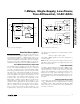
Figure 13. SPI/MICROWIRE Serial-Interface Timing—Continuous Conversion (CPOL = CPHA = 0), (CPOL = CPHA = 1)
0 0 0 D11 D10 D9 D8 D7 D6 D5 D4 D3 D2 D1 D0 0
DOUT
SCLK
CNVST
0
1
1
14
16
Figure 12. SPI/MICROWIRE Serial-Interface Timing—Single Conversion (CPOL = CPHA = 0), (CPOL = CPHA = 1)
Figure 14. QSPI Serial-Interface Timing—Single Conversion (CPOL = 1, CPHA = 1)
SCLK
DOUT
CNVST
16
D0
D1
D11
D10
D6D7D8 D5 D4 D3 D2
HIGH-Z
D9
HIGH-Z
2