
Datasheet


MAX1270/MAX1271
Multirange, +5V, 8-Channel,
Serial 12-Bit ADCs
8 _______________________________________________________________________________________
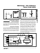
Pin Description
PIN
PDIP
SSOP
NAME FUNCTION
11 V
DD
+5V Supply. Bypass with a 0.1µF capacitor to AGND.
2, 4
2, 3 DGND Digital Ground
3, 9,
22, 24
4, 7, 8,
11, 22,
24, 25, 28
N.C. No Connection. No internal connection.
55SCLK
Serial Clock Input. Clocks data in and out of serial interface. In external clock mode, SCLK also
sets the conversion speed.
66 CS
Active-Low Chip-Select Input. Data is not clocked into DIN unless CS is low. When CS is high,
DOUT is high impedance.
79 DIN Serial Data Input. Data is clocked in on the rising edge of SCLK.
810
SSTRB
Serial Strobe Output. In internal clock mode, SSTRB goes low after the falling edge of the eighth
SCLK and returns high when the conversion is done. In external clock mode, SSTRB pulses high
for one clock period before the MSB decision. High impedance when CS is high in external
clock mode.
10
12 DOUT
Serial Data Output. Data is clocked out on the falling edge of SCLK. High impedance when CS is
high.
11
13 SHDN Shutdown Input. When low, device is in FULLPD mode. Connect high for normal operation.
12
14 AGND Analog Ground
13–20
15–21, 23 CH0–CH7
Analog Input Channels
21
26
REFADJ
Bandgap Voltage-Reference Output/External Adjust Pin. Bypass with a 0.01µF capacitor to AGND.
Connect to V
DD
when using an external reference at REF.
23
27 REF
Refer ence- Buffer O utp ut/AD C Refer ence Inp ut. In i nter nal r efer ence m od e, the r efer ence b uffer
p r ovi d es a 4.096V nom i nal outp ut, exter nal l y ad j ustab l e to RE FAD J. In exter nal r efer ence m od e,
d i sab l e the i nter nal r efer ence b y p ul l i ng RE FAD J to V
D D
and ap p l yi ng the exter nal r efer ence to RE F.
0
1
2
3
4
5
6
7
8
0.1 1 10 100 1000
AVERAGE SUPPLY CURRENT vs.
CONVERSION RATE (USING STANDBY)
MAX1270-toc10
CONVERSION RATE (ksps)
AVERAGE SUPPLY CURRENT (mA)
V
DD
= 5V, INTERNAL REFERENCE,
f
CLK
= 2MHz
EXTERNAL CLOCK MODE.
LOW-RANGE UNIPOLAR MODE.
V
CH_
= 0
0
1
2
3
4
5
6
7
8
0.1 1 10 100 1000
AVERAGE SUPPLY CURRENT vs.
CONVERSION RATE (USING FULLPD)
MAX1270-toc11
CONVERSION RATE (ksps)
AVERAGE SUPPLY CURRENT (mA)
V
DD
= 5V, INTERNAL REFERENCE,
f
CLK
= 2MHz
EXTERNAL CLOCK MODE.
LOW-RANGE UNIPOLAR MODE.
V
CH_
= 0
Typical Operating Characteristics (continued)
(Typical Operating Circuit, V
DD
= +5V; external reference mode, V
REF
= +4.096V; 4.7µF at REF; external clock, f
CLK
= 2MHz;
110ksps; T
A
= +25°C, unless otherwise noted.)