
Datasheet


MAX1270/MAX1271
Multirange, +5V, 8-Channel,
Serial 12-Bit ADCs
______________________________________________________________________________________ 15
Internal Reference
The internally trimmed 2.50V reference is amplified
through the REFADJ buffer to provide 4.096V at REF.
Bypass REF with a 4.7µF capacitor to AGND and
REFADJ with a 0.01µF capacitor to AGND (Figure 13a).
The internal reference voltage is adjustable to ±1.5%
(±65 LSBs) with the reference-adjust circuit of Figure 1.
External Reference
To use the REF input directly, disable the internal buffer
by tying REFADJ to V
DD
(Figure 13b). Using the
REFADJ input eliminates the need to buffer the refer-
ence externally. When a reference is applied at
REFADJ, bypass REFADJ with a 0.01µF capacitor to
AGND. Note that when an external reference is applied
at REFADJ, the voltage at REF is given by:
V
REF
= 1.6384 x V
REFADJ
(2.4 < V
REF
< 4.18)
(Figure 13c). At REF and REFADJ, the input impedance
is a minimum of 10kΩ for DC currents. During conver-
sions, an external reference at REF must be able to deliv-
er 400µA DC load currents and must have an output
impedance of 10Ω or less. If the reference has higher
output impedance or is noisy, bypass REF with a 4.7µF
capacitor to AGND as close to the chip as possible.
With an external reference voltage of less than 4.096V
at REF or less than 2.5V at REFADJ, the increase in the
ratio of RMS noise to the LSB value (full-scale / 4096)
results in performance degradation (loss of effective
bits).
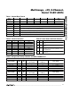
CS
SCLK
DIN
DOUT
A/D STATE
1
8
9
242214
16
START
SEL2 SEL1 SEL0
BIP
RNG
PD1 PD0
D11 D10 D9 D7D8 D6 D5 D4 D2D3 D1 D0
START
SEL2 SEL1 SEL0
BIP
RNG
PD1 PD0
START
SEL0SEL1SEL2
CONTROL BYTE Ø
RESULT Ø
CONTROL BYTE 1 CONTROL BYTE 2
13 SCLK
13 SCLK
SSTRB
D10D11 D9 D8 D6D7 D5 D4 D3
RESULT 1
ACQUISITION
CONVERSION
ACQUISITION
CONVERSION
HIGH-Z
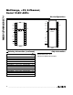
Figure 11. Internal Clock Mode—13 Clocks/Conversion Timing
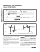
CS
SCLK
DIN
DOUT
A/D STATE
IDLE
9 24
25 32
16 17
START
START
SEL2 SEL1 SEL0 BIPRNG PD1 PD0
D11 D10 D9 D7D8 D6 D5 D4 D2D3 D1 D0
START
SEL2 SEL1 SEL0 BIPRNG PD1 PD0
CONTROL BYTE Ø
RESULT Ø
CONTROL BYTE 1 CB 2
16 SCLK
16 SCLK
SSTRB
D10
D11
D9 D8 D6D7 D5 D4 D3
RESULT 1
ACQUISITION CONVERSION ACQUISITION CONVERSION
HIGH-ZHIGH-Z HIGH-Z
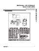
1
8
Figure 12. Internal Clock Mode—16 Clocks/Conversion Timing