
Datasheet


MAX1270/MAX1271
Multirange, +5V, 8-Channel,
Serial 12-Bit ADCs
______________________________________________________________________________________ 11
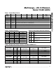
Table 1. Control-Byte Format
BIT 7
(MSB)
BIT 6 BIT 5 BIT 4 BIT 3 BIT 2 BIT 1
BIT 0
(LSB)
START SEL2 SEL1 SEL0 RNG BIP PD1 PD0
BIT NAME DESCRIPTION
7 (MSB) START First logic 1 after CS goes low defines the beginning of the control byte.
6, 5, 4
SEL2, SEL1,
SEL0
These 3 bits select the desired “on” channel (Table 2).
3 RNG Selects the full-scale input voltage range (Table 3).
2 BIP Selects the unipolar or bipolar conversion mode (Table 3).
1, 0 (LSB) PD1, PD0 Select clock and power-down modes (Table 4).
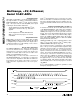
Table 2. Channel Selection
SEL2 SEL1 SEL0 CHANNEL
000 CH0
001 CH1
010 CH2
011 CH3
100 CH4
101 CH5
110 CH6
111 CH7
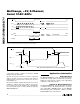
Table 4. Power-Down and Clock Selection
PD1
PD0
MODE
00
Normal operation (always on), internal clock
mode.
01
Normal operation (always on), external clock
mode.
10
Standby power-down mode (STBYPD), clock
mode unaffected.
11
Full power-down mode (FULLPD), clock mode
unaffected.
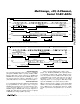
Table 3. Range and Polarity Selection for MAX1270/MAX1271
RANGE AND POLARITY SELECTION FOR THE MAX1270
INPUT RANGE RNG BIP
Negative
FULL SCALE
ZERO
SCALE (V)
FULL SCALE
0 to +5V 0 0 — 0 V
REF
x 1.2207
0 to +10V 1 0 — 0 V
REF
x 2.4414
±5V 0 1 -V
REF
x 1.2207 0 V
REF
x 1.2207
±10V 1 1 -V
REF
x 2.4414 0 V
REF
x 2.4414
RANGE AND POLARITY SELECTION FOR THE MAX1271
INPUT RANGE RNG BIP
Negative
FULL SCALE
ZERO
SCALE (V)
FULL SCALE
0 to V
REF
/2 0 0 — 0 V
REF
/2
0 to V
REF
10 — 0 V
REF
±V
REF
/2 0 1 -V
REF
/2 0 V
REF
/2
±V
REF
11 -V
REF
0V
REF