
Datasheet


MAX1236–MAX1239
2.7V to 3.6V and 4.5V to 5.5V, Low-Power,
4-/12-Channel, 2-Wire Serial, 12-Bit ADCs
_______________________________________________________________________________________ 5
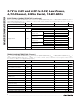
PARAMETER SYMBOL CONDITIONS MIN TYP MAX UNITS
TIMING CHARACTERISTICS FOR HIGH-SPEED MODE (C
B
= 400pF, Note 12)
Serial Clock Frequency f
SCLH
(Note 13) 1.7 MHz
Hold Time, Repeated START
Condition (Sr)
t
HD
,
STA
160 ns
Low Period of the SCL Clock t
LOW
320 ns
High Period of the SCL Clock t
HIGH
120 ns
Setup Time for a Repeated START
Condition (Sr)
t
SU
,
STA
160 ns
Data Hold Time t
HD
,
DAT
(Note 10) 0 150 ns
Data Setup Time t
SU
,
DAT
10 ns
Rise Time of SCL Signal
(Current Source Enabled)
t
RCL
20 80 ns
Rise Time of SCL Signal after
Acknowledge Bit
t
RCL1
Measured from 0.3V
DD
- 0.7V
DD
20 160 ns
Fall Time of SCL Signal t
FCL
Measured from 0.3V
DD
- 0.7V
DD
20 80 ns
Rise Time of SDA Signal t
RDA
Measured from 0.3V
DD
- 0.7V
DD
20 160 ns
Fall Time of SDA Signal t
FDA
Measured from 0.3V
DD
- 0.7V
DD
(Note 11) 20 160 ns
Setup Time for STOP (P) Condition t
SU
,
STO
160 ns
Capacitive Load for Each Bus Line C
B
400 pF
Pulse Width of Spike Suppressed t
SP
(Notes 10 and 13) 0 10 ns
TIMING CHARACTERISTICS (Figure 1) (continued)
(V
DD
= 2.7V to 3.6V (MAX1237/MAX1239), V
DD
= 4.5V to 5.5V (MAX1236/MAX1238), V
REF
= 2.048V (MAX1237/MAX1239), V
REF
=
4.096V (MAX1236/MAX1238), f
SCL
= 1.7MHz, T
A
= T
MIN
to T
MAX
, unless otherwise noted. Typical values are at
T
A
= +25°C, see Tables 1–5 for programming notation.)
Note 1: For DC accuracy, the MAX1236/MAX1238 are tested at V
DD
= 5V and the MAX1237/MAX1239 are tested at V
DD
= 3V. All
devices are configured for unipolar, single-ended inputs.
Note 2: Relative accuracy is the deviation of the analog value at any code from its theoretical value after the full-scale range and
offsets have been calibrated.
Note 3: Offset nulled.
Note 4: Conversion time is defined as the number of clock cycles needed for conversion multiplied by the clock period. Conversion
time does not include acquisition time. SCL is the conversion clock in the external clock mode.
Note 5: A filter on the SDA and SCL inputs suppresses noise spikes and delays the sampling instant.
Note 6: The absolute input-voltage range for the analog inputs (AIN0–AIN11) is from GND to V
DD
.
Note 7: When the internal reference is configured to be available at AIN_/REF (SEL[2:1] = 11) decouple AIN_/REF to GND with a
0.1µF capacitor and a 2kΩ series resistor (see the
Typical Operating Circuit
).
Note 8: ADC performance is limited by the converter’s noise floor, typically 300µV
P-P
.
Note 9: Measured as for the MAX1237/MAX1239
VVVV
V
VV
FS FS
REF
N
(. ) (. )
(. . )
36 27
21
36 27
−
−
−
[]
×
⎡
⎣
⎢
⎢
⎤
⎦
⎥
⎥