
Datasheet


Note 1: These tests are performed at V
DD
= 5V, V
SS
= -15V. Operation over supply is guaranteed by supply rejection tests.
Note 2: Ideal full-scale transition is at +5V - 3/2 LSB = +4.9963V, adjusted for offset error.
Note 3: Supply rejection defined as change in full-scale transition voltage with the specified change in supply voltage = (FS at nomi-
nal supply)- (FS at nominal supply ± tolerance), expressed in LSBs.
Note 4: For design guidance only, not tested.
Note 5: Temperature drift is defined as the change in output voltage from +25°C to T
MIN
or T
MAX
. It is calculated as T
C
= ΔV
REF
/
V
REF
/(ΔT).
Note 6: V
CS
= V
RD
= V
CONVST
= 0V, V
MODE
= 5V.
Note 7: Control inputs specified with t
r
= t
f
= 5ns ( 10% to 90% of +5V) and timed from a 1.6V voltage level. Output delays are
measured to +0.8V if going low, or +2.4V if going high. For bus-relinquish time, a change of 0.5V is measured. See Figures
1 and 2 for load circuits.
Note 8: For design guidance only, not tested.
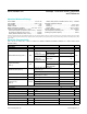
(V
DD
= +5V, V
SS
= -12V to -15V, 100% tested, T
A
= T
MIN
to T
MAX
, unless otherwise noted.) (Note 7)
PARAMETER SYMBOL CONDITIONS
T
A
= +25°C MAX12_C/E
UNITS
MIN TYP MAX MIN TYP MAX
CS to RD Setup Time t
CS
0 0 ns
CS to RD Hold Time t
CH
0 0 ns
CONVST Pulse Width t
CW
30 30 ns
RD Pulse Width t
RW
t
DA
t
DA
ns
Data-Access Time t
DA
C
L
= 100pF 40 75 100 ns
Bus-Relinquish Time t
DH
30 50 65 ns
RD or CONVST to BUSY t
B0
C
L
= 50pF 30 75 100 ns
CLKIN to BUSY or INT
t
B1
C
L
= 50pF 70 110 150 ns
CLKIN to BUSY Low
t
B2
In mode 5 45 90 120 ns
RD to INT High t
IH
C
L
= 50pF 30 50 75 ns
BUSY or INT to Data Valid t
BD
C
L
(Data) = 100pF,
C
L
(INT, BUSY) = 50pF
20 30 ns
Acquisition Time (Note 8) t
ACQ
350 350 ns
Aperture Delay (Note 8) t
AP
10 ns
Aperture Jitter (Note 8) 30 ps
PIN NAME FUNCTION
1 MODE
Mode Input. Hardwire to set operational mode.
V
DD
: Single conversion, INT Output
OPEN: Single conversion, BUSY Output
DGND: Continuous conversions, BUSY Output
2 V
SS
Negative Power Supply, -12V or -15V
3 V
DD
Positive Power Supply, +5V
4 AIN Sampling Analog Input, ±5V bipolar input range
5 V
REF
-5V Reference Output. Bypass to AGND with 22µF || 0.1µF.
MAX120/MAX122 500ksps, 12-Bit ADCs with Track/Hold
and Reference
www.maximintegrated.com
Maxim Integrated
│
4
Timing Characteristics
Pin Description