
Datasheet


V
DD
to DGND .......................................................... -0.3V to +6V
V
SS
to DGND ........................................................+0.3V to -17V
AIN to AGND .......................................................................±15V
AGND to DGND .................................................................±0.3V
Digital Inputs/Outputs to DGND ....................-0.3V to (V + 0.3V)
Continuous Power Dissipation (T
A
= +70°C)
Narrow PDIP (derate 13.33mW/°C above +70°C) ....1067mW
SO (derate 11.76mW/°C above +70°C) ......................941mW
SSOP (derate 8.00mW/°C above +70°C) ...................640mW
Narrow CDIP (derate 12.50mW/°C above +70°C) ....1000mW
Operating Temperature Ranges
MAX12_C ...........................................................0°C to +70°C
MAX12_E_ .................................................... -40°C to +85°C
MAX12_MRG .............................................. -55°C to +125°C
Storage Temperature Range ..............................-65°C to+160°C
Lead Temperature (soldering, 10s) .................................+300°C
Soldering Temperature (reflow) ....................................... +260°C
(V
DD
= +4.75V to +5.25V, V
SS
= -10.8V to -15.75V, f
CLK
= 8MHz for MAX120 and 5MHz for MAX122, T
A
= T
MIN
to T
MAX
, unless
otherwise noted.)
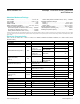
PARAMETER SYMBOL CONDITIONS MIN TYP MAX UNITS
ACCURACY
Resolution RES 12 Bits
Differential Nonlinearity (Note 1) DNL
12-bit no missing
codes over
temperature range
MAX122AC/AE ±3/4
LSB
MAX120C/E,
MAX122BC/BE
±1
11-bit no missing
codes over
temperature range
MAX120M ±2
Integral Nonlinearity
(Note 1)
INL
MAX122AC/AE ±3/4
LSB
MAX120C/E,
MAX122BC/BE
±1
Bipolar Zero Error (Note 1)
Code 00..00 to 00..01 transition,
near V
AIN
= 0V
±3 LSB
Temperature drift ±0.005
LSB/”C
Full-Scale Error (Notes 1, 2)
Including reference; adjusted for bipolar
zero error; T
A
= +25°C
±8 LSB
Full-Scale Temperature Drift Excluding reference ±1
ppm/”C
Power-Supply Rejection Ratio
(Change in FS)
(Note 3)
PSRR
V
DD
only, 5V ±5% ±1/4 ±3/4
LSBV
SS
only, -12V ±10% ±1/4 ±1
V
SS
only, -15V ±5% ±1/4 ±1
ANALOG INPUT
Input Range -5 +5 V
Input Current V
AIN
= +5V (approximately 6kΩ to REF) 2.5 mA
Input Capacitance (Note 4) 10 pF
Full-Power Input Bandwidth 1.5 MHz
REFERENCE
Output Voltage No external load, V
AIN
= 5V, T
A
= +25°C -5 02 -4.98 V
External Load Regulation 0mA < I
SINK
< 5mA, V
AIN
= 0V 5 mV
Temperature Drift (Note 5) MAX12_C/E ±25
ppm/°C
MAX120/MAX122 500ksps, 12-Bit ADCs with Track/Hold
and Reference
www.maximintegrated.com
Maxim Integrated
│
2
Absolute Maximum Ratings
Stresses beyond those listed under “Absolute Maximum Ratings” may cause permanent damage to the device. These are stress ratings only, and functional operation of the device at these
or any other conditions beyond those indicated in the operational sections of the specifications is not implied. Exposure to absolute maximum rating conditions for extended periods may affect
device reliability.
Electrical Characteristics