
Datasheet


MAX1178/MAX1188
Power-Down Modes
Select standby mode or shutdown mode with the R/C
bit during the second falling edge of CS (see the
Selecting Standby or Shutdown Mode section). The
MAX1178/MAX1188 automatically enter either standby
mode (reference and buffer on) or shutdown (reference
and buffer off) after each conversion, depending on the
status of R/C during the second falling edge of CS.
Internal Clock
The MAX1178/MAX1188 generate an internal conver-
sion clock to free the µP from the burden of running the
SAR conversion clock. Total conversion time (t
CONV
)
after entering hold mode (second falling edge of CS) to
end-of-conversion (EOC) falling is 4.7µs (max).
Applications Information
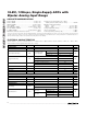
Starting a Conversion
CS and R/C control acquisition and conversion in the
MAX1178/MAX1188 (Figure 2). The first falling edge of
CS powers up the device and puts it in acquire mode if
R/C is low. The convert start is ignored if R/C is high.
The MAX1178/MAX1188 need at least 12ms for the
internal reference to wake up and settle before starting
the conversion (C
REFADJ
= 0.1µF, C
REF
= 10µF), if
powering up from shutdown.
16-Bit, 135ksps, Single-Supply ADCs with
Bipolar Analog Input Range
8 _______________________________________________________________________________________
CS
R/C
REF POWER-
DOWN CONTROL
EOC
t
ACQ
t
CONV
t
CSH
t
CSL
t
DH
t
DO
t
EOC
t
DS
t
DV
HBEN
D7/D15–D0/D8
HIGH/LOW
BYTE VALID
HIGH/LOW
BYTE VALID
t
DO
t
DO1
HIGH-Z
t
BR
HIGH-Z
Figure 2. MAX1178/MAX1188 Timing Diagram
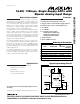
D0–D7
OR
D8–D15
µ
P DATA
BUS
AV
DD
DV
DD
AGND DGND
+5V ANALOG +5V DIGITAL
ANALOG INPUT AIN
HBEN
EOC
CS
R/C
REF
REFADJ
HIGH
BYTE
LOW
BYTE
10
µ
F
0.1
µ
F
0.1
µ
F
0.1
µ
F
MAX1178
MAX1188
Figure 3. Typical Operating Circuit for the MAX1178/MAX1188