
Datasheet


MAX1167/MAX1168
Multichannel, 16-Bit, 200ksps Analog-to-Digital
Converters
26 ______________________________________________________________________________________
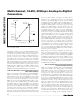
DOUT*
CS
SCLK
1ST BYTE READ
2ND BYTE READ
*WHEN CS IS HIGH, DOUT = HIGH-Z
MSB
HIGH-Z
3RD BYTE READ
LSB
D1 D0D7 D6 D5 D4 D3 D2
24
20
16128641
D15
D14 D13 D12 D11 D10 D9 D8
00000000
Figure 22b. SPI Interface Timing with PIC16/PIC17 in Master Mode (CKE = 1, CKP = 0, SMP = 0, SSPM3 - SSPM0 = 0001)
Serial Interfaces
SPI and MICROWIRE Interfaces
When using the SPI (Figure 20a) or MICROWIRE (Figure
20b) interfaces, set CPOL = 0 and CPHA = 0. Drive CS
low to power on the MAX1167/MAX1168 before starting a
conversion (Figure 20c). Three consecutive 8-bit-wide
readings are necessary to obtain the entire 16-bit result
from the ADC. DOUT data transitions on the serial clock’s
falling edge. The first 8-bit-wide data stream contains all
leading zeros. The 2nd 8-bit-wide data stream contains
the MSB through D6. The 3rd 8-bit-wide data stream con-
tains D5 through D0 followed by S1 and S0.
QSPI Interface
Using the high-speed QSPI interface with CPOL = 0 and
CPHA = 0, the MAX1167/MAX1168 support a maximum
f
SCLK
of 4.8MHz. Figure 21a shows the MAX1167/
MAX1168 connected to a QSPI master, and Figure 21b
shows the associated interface timing.
PIC16 with SSP Module and PIC17
Interface
The MAX1167/MAX1168 are compatible with a
PIC16/PIC17 controller (µC), using the synchronous seri-
al-port (SSP) module.
To establish SPI communication, connect the controller
as shown in Figure 22a and configure the PIC16/PIC17
as system master by initializing its synchronous serial-
port control register (SSPCON) and synchronous serial-
port status register (SSPSTAT) to the bit patterns shown
in Tables 7 and 8.
In SPI mode, the PIC16/PIC17 µCs allow 8 bits of data to
be synchronously transmitted and received simultane-
ously. Three consecutive 8-bit-wide readings (Figure
22b) are necessary to obtain the entire 16-bit result from
the ADC. DOUT data transitions on the serial clock’s
falling edge and is clocked into the µC on SCLK’s rising
edge. The first 8-bit-wide data stream contains all zeros.
The 2nd 8-bit-wide data stream contains the MSB
through D6. The 3rd 8-bit-wide data stream contains bits
D5 through D0 followed by S1 and S0.
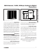
DSP
EXTERNAL
CLOCK
SCLK
DSPR
DSPX
DIN
DOUT
SCLK
TFS
RFS
DT
DR
FL1
CS
MAX1168
Figure 23. DSP Interface Connection