
Datasheet


MAX1167/MAX1168
Digital Interface
The MAX1167/MAX1168 feature an SPI/QSPI/
MICROWIRE-compatible, 3-wire serial interface. The
MAX1167 digital interface consists of digital inputs CS,
SCLK, and DIN and outputs DOUT and EOC. The
MAX1167 operates in the following modes:
• SPI interface with external clock
• SPI interface with internal clock
• SPI interface with internal clock and scan mode
In addition to the standard 3-wire serial interface modes,
the MAX1168 includes a DSPR input and a DSPX output
for communicating with DSPs in external clock mode and
a DSEL input to determine 8-bit-wide or 16-bit-wide data-
transfer mode. When not using the MAX1168 in the DSP
interface mode, connect DSPR to DV
DD
and leave DSPX
unconnected.
Command/Configuration/Control Register
Table 1 shows the contents of the command/configura-
tion/control register and the state of each bit after initial
power-up. Tables 2–6 define the control and configuration
of the device for each bit. Cycling the power supplies
resets the command/configuration/control register to the
power-on-reset default state.
Initialization After Power-Up
A logic high on CS places the MAX1167/MAX1168 in
the shutdown mode chosen by the power-down bits,
and places DOUT in a high-impedance state. Drive CS
low to power up and enable the MAX1167/MAX1168
before starting a conversion. In internal reference
mode, allow 5ms for the shutdown internal reference
and/or buffer to wake and stabilize before starting a
conversion. In external reference mode (or if the inter-
nal reference is already on), no reference settling time
is needed after power-up.
Multichannel, 16-Bit, 200ksps Analog-to-Digital
Converters
14 ______________________________________________________________________________________
SCLK
DOUT
AGND
DGND
AIN0
REF
AV
DD
DV
DD
DOUT
SCLK
CS
+5V
DIN
ANALOG
INPUTS
+5V
1μF
0.1μF
0.1μF
GND
MAX1167
0.1μF
AIN1
AIN2
AIN3
DIN
EOC
EOC
AGND
REFCAP
CS
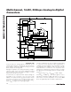
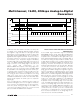
Figure 5. MAX1167 Typical Operating Circuit
SCLK
DOUT
AGND
DGND
AIN0
REF
AV
DD
DV
DD
DOUT
SCLK
CS
+5V
16
8
DIN
ANALOG
INPUTS
+5V
1μF
0.1μF
0.1μF
GND
MAX1168
0.1μF
AIN1
AIN2
AIN3
AIN4
AIN5
AIN6
AIN7
DIN
DSEL
DSPR
DSPX
DSPX
EOC
AGND
REFCAP
EOC
CS
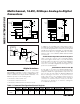
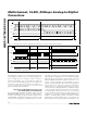
Figure 6. MAX1168 T ypical Operating Circuit
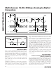
AUTOZERO
RAIL
CAPACITIVE
DAC
C
DAC
REF
AGND
TRACK
HOLD
HOLD TRACK
ZERO
MUX
R
IN
R
DSON
AIN_
C
MUX
C
SWITCH
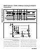
Figure 7. Equivalent Input Circuit
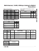
BIT7 (MSB) BIT6 BIT5 BIT4 BIT3 BIT2 BIT1 BIT0 (LSB)
COMMAND
CH SEL2 CH SEL1 CH SEL0 SCAN1 SCAN0 REF/PD_SEL1 REF/PD SEL0 INT/EXT CLK
POWER-UP
STATE
00000110
Table 1. Command/Configuration/Control Register