
Datasheet


MAX1165/MAX1166
Low-Power, 16-Bit Analog-to-Digital Converter
with Parallel Interface
8 _______________________________________________________________________________________
Detailed Description
Converter Operation
The MAX1165/MAX1166 use a successive-approxima-
tion (SAR) conversion technique with an inherent track-
and-hold (T/H) stage to convert an analog input into a
16-bit digital output. Parallel outputs provide a high-
speed interface to most microprocessors (µPs). The
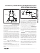
Functional Diagram
shows a simplified internal archi-
tecture of the MAX1165/MAX1166. Figure 3 shows a
typical application circuit for the MAX1166.
Analog Input
The equivalent input circuit is shown in Figure 4. A
switched capacitor digital-to-analog converter (DAC)
provides an inherent T/H function. The single-ended
input is connected between AIN and AGND.
Input Bandwidth
The ADC’s input-tracking circuitry has a 4MHz small-
signal bandwidth, so it is possible to digitize high-
speed transient events and measure periodic signals
with bandwidths exceeding the ADC’s sampling rate by
using undersampling techniques. To avoid aliasing of
unwanted high-frequency signals into the frequency
band of interest, use anti-alias filtering.
Analog Input Protection
Internal protection diodes, which clamp the analog
input to AV
DD
and/or AGND, allow the input to swing
from AGND - 0.3V to AV
DD
+ 0.3V, without damaging
the device.
If the analog input exceeds 300mV beyond the sup-
plies, limit the input current to 10mA.
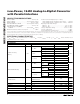
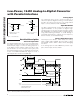
D0–D15 D0–D15
1mA
DGND
DGND
DV
DD
C
LOAD
= 20pF
C
LOAD
= 20pF
a) HIGH-Z TO V
OH
, V
OL
TO V
OH
,
AND V
OH
TO HIGH-Z
b) HIGH-Z TO V
OL
, V
OH
TO V
OL
,
AND V
OL
TO HIGH-Z
1mA
Figure 1. Load Circuits
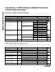
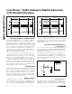
CS
R/C
REF POWER-
DOWN BIT
EOC
D0–D15
HBEN*
DATA VALID
D8/D15–
D0/D7*
HIGH-/LOW-
BYTE VALID
HIGH-/LOW-
BYTE VALID
t
ACQ
t
CONV
t
CSH
t
CSL
t
DH
t
DO
t
DO1
t
BR
*HBEN AND BYTE-WIDE DATA BUS
AVAILABLE ON MAX1166 ONLY.
t
DS
t
DV
t
EOC
HIGH-Z
HIGH-Z
t
BR
Figure 2. MAX1165/MAX1166 Timing Diagram