
Datasheet


MAX1165/MAX1166
Low-Power, 16-Bit Analog-to-Digital Converter
with Parallel Interface
4 _______________________________________________________________________________________
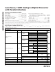
ELECTRICAL CHARACTERISTICS (continued)
(AV
DD
= DV
DD
= +5V, external reference = +4.096V, C
REF
= 4.7µF, C
REFADJ
= 0.1µF, T
A
= T
MIN
to T
MAX
, unless otherwise noted.
Typical values are at T
A
= +25°C.)
PARAMETER SYMBOL CONDITIONS MIN TYP MAX UNITS
Three-State Output Capacitance C
OZ
15 pF
POWER REQUIREMENTS
Analog Supply Voltage AV
DD
4.75 5.25 V
Digital Supply DV
DD
2.7 AV
DD
V
165ksps 3.2 3.6
100ksps 2.6
10ksps 1.9
Internal reference
1ksps 1.8
165ksps 2.4 2.8
100ksps 1.8
10ksps 0.8
Analog Supply Current I
AVDD
External reference
1ksps 0.08
mA
165ksps 0.5 0.7
100ksps 0.3
10ksps 0.03
Digital Supply Current I
DVDD
D0–D15 = all zeros
1ksps 0.003
mA
I
AVDD
0.5 5
Full power-down
I
DVDD
0.5 6
µA
I
AVDD
1.0 1.2 mAShutdown Supply Current I
SHDN
REF and REF buffer enabled
(standby mode)
I
DVDD
(Note 4)
0.5 5 µA
Power-Supply Rejection Ratio
PSRR AV
DD
= +5V ±5%, full-scale input (Note 5) 68 dB
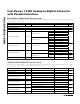
TIMING CHARACTERISTICS (Figures 1 and 2)
(AV
DD
= +4.75V to +5.25V, DV
DD
= +2.7V to AV
DD
, external reference = +4.096V, C
REF
= 4.7µF, C
REFADJ
= 0.1µF, C
LOAD
= 20pF,
T
A
= T
MIN
to T
MAX
, unless otherwise noted. Typical values are at T
A
= +25°C.)
PARAMETER SYMBOL CONDITIONS MIN TYP MAX UNITS
Acquisition Time t
ACQ
1.1
Conversion Time t
CONV
4.7
µs
CS Pulse Width High t
CSH
(Note 6) 40 ns
V
DVDD
= 4.75V to 5.25V 40
CS Pulse Width Low (Note 6) t
CSL
V
DVDD
= 2.7V to 5.25V 60
ns
R/C to CS Fall Setup Time t
DS
0ns
V
DVDD
= 4.75V to 5.25V 40
R/C to CS Fall Hold Time t
DH
V
DVDD
= 2.7V to 5.25V 60
ns
V
DVDD
= 4.75V to 5.25V 40
CS to Output Data Valid t
DO
V
DVDD
= 2.7V to 5.25V 80
ns
V
DVDD
= 4.75V to 5.25V 40
HBEN Transition to Output Data
Valid (MAX1166 Only)
t
DO1
V
DVDD
= 2.7V to 5.25V 80
ns
EOC Fall to CS Fall t
DV
0ns