
Datasheet


6 ______________________________________________________________________________________
MAX11661–MAX11666
500ksps, Low-Power,
Serial 12-/10-/8-Bit ADCs
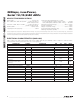
ELECTRICAL CHARACTERISTICS (MAX11665) (continued)
(V
DD
= 2.2V to 3.6V, f
SCLK
= 8MHz, 50% duty cycle, 500ksps, C
DOUT
= 10pF,
T
A
= -40NC to +125NC, unless otherwise noted. Typical
values are at T
A
= +25NC.) (Note 1)
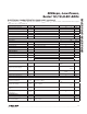
ELECTRICAL CHARACTERISTICS (MAX11664)
(V
DD
= 2.2V to 3.6V, V
REF
= V
DD
, V
OVDD
= V
DD
, f
SCLK
= 8MHz, 50% duty cycle, 500ksps; C
DOUT
= 10pF,
T
A
= -40NC to +125NC,
unless otherwise noted. Typical values are at T
A
= +25NC.) (Note 1)
PARAMETER SYMBOL CONDITIONS MIN TYP MAX UNITS
Positive Supply Current (Full-
Power Mode), No Clock
I
VDD
1.48 mA
Power-Down Current I
PD
Leakage only 1.3 10
FA
Line Rejection V
DD
= 2.2V to 3.6V 0.7 LSB/V
TIMING CHARACTERISTICS (Note 2)
Quiet Time t
Q
(Note 3) 4 ns
CS Pulse Width
t
1
(Note 3) 10 ns
CS Fall to SCLK Setup
t
2
(Note 3) 5 ns
CS Falling Until DOUT High-
Impedance Disabled
t
3
(Note 3) 1 ns
Data Access Time After SCLK
Falling Edge
t
4
Figure 2, V
DD
= 2.2V to 3.6V 15 ns
SCLK Pulse Width Low t
5
Percentage of clock period (Note 3) 40 60 %
SCLK Pulse Width High t
6
Percentage of clock period (Note 3) 40 60 %
Data Hold Time From SCLK
Falling Edge
t
7
Figure 3 5 ns
SCLK Falling Until DOUT High
Impedance
t
8
Figure 4 (Note 3) 2.5 14 ns
Power-Up Time Conversion cycle (Note 3) 1 Cycle
PARAMETER SYMBOL CONDITIONS MIN TYP MAX UNITS
DC ACCURACY
Resolution 10 Bits
Integral Nonlinearity INL
Q0.5
LSB
Differential Nonlinearity DNL No missing codes
Q0.5
LSB
Offset Error OE
Q0.5 Q1.3
LSB
Gain Error GE Excluding offset and reference errors
0
Q1.3
LSB
Total Unadjusted Error TUE
Q0.5
LSB
Channel-to-Channel Offset
Matching
Q0.1
LSB
Channel-to-Channel Gain
Matching
Q0.05
LSB
DYNAMIC PERFORMANCE (f
AIN
= 250kHz)
Signal-to-Noise and Distortion SINAD 60.5 61.6 dB
Signal-to-Noise Ratio SNR 60.5 61.6 dB
Total Harmonic Distortion THD -83 -73 dB
Spurious-Free Dynamic Range SFDR 75 dB