
Datasheet


______________________________________________________________________________________ 25
MAX11661–MAX11666
500ksps, Low-Power,
Serial 12-/10-/8-Bit ADCs
and stays within a given error band centered on the
resulting steady-state amplifier output level. The ADC
input sampling capacitor charges during the sampling
cycle, referred to as the acquisition period. During this
acquisition period, the settling time is affected by the
input resistance and the input sampling capacitance.
This error can be estimated by looking at the settling of
an RC time constant using the input capacitance and
the source impedance over the acquisition time period.
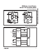
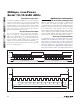
Figure 15 shows a typical application circuit. The
MAX4430, offering a settling time of 37ns at 16 bits, is
an excellent choice for this application. See the THD
vs. Input Resistance graph in the Typical Operating
Characteristics.
Choosing a Reference
For devices using an external reference, the choice of
the reference determines the output accuracy of the
ADC. An ideal voltage reference provides a perfect initial
accuracy and maintains the reference voltage indepen-
dent of changes in load current, temperature, and time.
Considerations in selecting a reference include initial
voltage accuracy, temperature drift, current source,
sink capability, quiescent current, and noise. Figure 15
shows a typical application circuit using the MAX6126
to provide the reference voltage. The MAX6033 and
MAX6043 are also excellent choices.
Figure 15. Typical Application Circuit
MAX11662
MAX11664
MAX11666
MAX6126
OVDD
V
OVDD
3V
SCLK
CPU
DOUT
CHSEL
SCK
MISO
CS SS
0.1µF
1µF
10µF
0.1µF
AGND
AIN1
AIN1
V
DC
4
1
5
2
2
3
AIN2
V
DD
72
1
6
4
3
10µF
0.1µF
0.1µF
0.1µF
+5V
-5V
470pF
C0G CAPACITOR
10I
500I
470pF
C0G CAPACITOR
10µF
+5V
10µF
0.1µF
0.1µF 10µF
REF
OUTF IN
NR
OUTS
GNDS
GND
EP
MAX4430
AIN2
V
DC
4
1
5
3
0.1µF
+5V
-5V
10I
10µF
0.1µF 10µF
MAX4430
500I
500I
500I
100pF C0G
100pF C0G