
Datasheet


24 _____________________________________________________________________________________
MAX11661–MAX11666
500ksps, Low-Power,
Serial 12-/10-/8-Bit ADCs
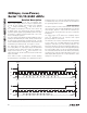
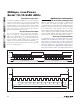
Figure 13. Channel Select Timing Diagram
Dual-Channel Operation
The MAX11662/MAX11664/MAX11666 feature dual-input
channels. These devices use a channel-select (CHSEL)
input to select between analog input AIN1 (CHSEL = 0)
or AIN2 (CHSEL = 1). As shown in Figure 13, the CHSEL
signal is required to change between the 2nd and 12th
clock cycle within a regular conversion to guarantee
proper switching between channels.
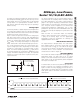
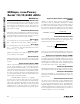
14-Cycle Conversion Mode
The ICs can operate with 14 cycles per conversion.
Figure 14 shows the corresponding timing diagram.
Observe that DOUT does not go into high-impedance
mode. Also, observe that t
ACQ
needs to be sufficiently
long to guarantee proper settling of the analog input
voltage. See the Electrical Characteristics table for t
ACQ
requirements and the Analog Input section for a descrip-
tion of the analog inputs.
Applications Information
Layout, Grounding, and Bypassing
For best performance, use PCBs with a solid ground
plane. Ensure that digital and analog signal lines are
separated from each other. Do not run analog and digital
(especially clock) lines parallel to one another or digital
lines underneath the ADC package. Noise in the V
DD
power supply, OVDD, and REF affects the ADC’s perfor-
mance. Bypass the V
DD
, OVDD, and REF to ground with
0.1FF and 10FF bypass capacitors. Minimize capacitor
lead and trace lengths for best supply-noise rejection.
Choosing an Input Amplifier
It is important to match the settling time of the input
amplifier to the acquisition time of the ADC. The conver-
sion results are accurate when the ADC samples the
input signal for an interval longer than the input signal’s
worst-case settling time. By definition, settling time is
the interval between the application of an input voltage
step and the point at which the output signal reaches
Figure 14. 14-Clock Cycle Operation
1
DATA CHANNEL AIN1 DATA CHANNEL AIN2
SCLK
CHSEL
DOUT
CS
2345678910111213141516 12345678910111213141516
1
DOUT
SCLK
(MSB)
SAMPLE
SAMPLE
1/f
SAMPLE
t
ACQ
t
CONVERT
CS
234
D10D11
5678910111213141
D9 D8 D7 D6 D5 D4 D3 D2 D1 D0 000