
Datasheet


______________________________________________________________________________________ 13
MAX11661–MAX11666
500ksps, Low-Power,
Serial 12-/10-/8-Bit ADCs
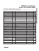
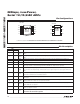
ELECTRICAL CHARACTERISTICS (MAX11661)
(V
DD
= 2.2V to 3.6V. f
SCLK
= 8MHz, 50% duty cycle, 500ksps. C
DOUT
= 10pF,
T
A
= -40NC to +125NC, unless otherwise noted. Typical
values are at T
A
= +25NC.) (Note 1)
PARAMETER SYMBOL CONDITIONS MIN TYP MAX UNITS
DC ACCURACY
Resolution 8 Bits
Integral Nonlinearity INL
Q0.25
LSB
Differential Nonlinearity DNL No missing codes
Q0.25
LSB
Offset Error OE
Q0.45 Q0.8
LSB
Gain Error GE Excluding offset and reference errors
Q0.04 Q0.5
LSB
Total Unadjusted Error TUE
Q0.75
LSB
DYNAMIC PERFORMANCE (f
AIN
= 250kHz)
Signal-to-Noise and Distortion SINAD 49 49.5 dB
Signal-to-Noise Ratio SNR 49 49.5 dB
Total Harmonic Distortion THD -70 -67 dB
Spurious-Free Dynamic Range SFDR 63 66 dB
Intermodulation Distortion IMD f
1
= 239.8kHz, f
2
= 200.2kHz -65 dB
Full-Power Bandwidth -3dB point 40 MHz
Full-Linear Bandwidth SINAD > 49dB 2.5 MHz
Small-Signal Bandwidth 45 MHz
CONVERSION RATE
Throughput 5 500 ksps
Conversion Time 1.56
Fs
Acquisition Time t
ACQ
52 ns
Aperture Delay
From CS falling edge
4 ns
Aperture Jitter 15 ps
Serial-Clock Frequency f
CLK
0.08 8 MHz
ANALOG INPUT (AIN)
Input Voltage Range V
AIN
0 V
DD
V
Input Leakage Current I
ILA
0.002
Q1 FA
Input Capacitance C
AIN
Track 20
pF
Hold 4
DIGITAL INPUTS (SCLK, CS)
Digital Input High Voltage V
IH
0.75 x
V
VDD
V
Digital Input Low Voltage V
IL
0.25 x
V
VDD
V
Digital Input Hysteresis V
HYST
0.15
V
VDD
V
Digital Input Leakage Current I
IL
Inputs at GND or V
DD
0.001
Q1 FA
Digital Input Capacitance C
IN
2 pF