
Datasheet


______________________________________________________________________________________ 11
MAX11661–MAX11666
500ksps, Low-Power,
Serial 12-/10-/8-Bit ADCs
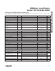
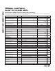
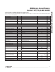
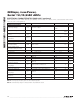
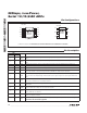
ELECTRICAL CHARACTERISTICS (MAX11662)
(V
DD
= 2.2V to 3.6V, V
REF
= V
DD
, V
OVDD
= V
DD
, f
SCLK
= 8MHz, 50% duty cycle, 500ksps, C
DOUT
= 10pF,
T
A
= -40NC to +125NC,
unless otherwise noted. Typical values are at T
A
= +25NC.) (Note 1)
PARAMETER SYMBOL CONDITIONS MIN TYP MAX UNITS
DC ACCURACY
Resolution 8 Bits
Integral Nonlinearity INL
Q0.25
LSB
Differential Nonlinearity DNL No missing codes
Q0.25
LSB
Offset Error OE 0.45
Q0.8
LSB
Gain Error GE Excluding offset and reference errors 0
Q0.25
LSB
Total Unadjusted Error TUE 0.5 LSB
Channel-to-Channel Offset
Matching
0.01 LSB
Channel-to-Channel Gain
Matching
0.01 LSB
DYNAMIC PERFORMANCE (f
AIN
= 250kHz)
Signal-to-Noise and Distortion SINAD 49 49.7 dB
Signal-to-Noise Ratio SNR 49 49.7 dB
Total Harmonic Distortion THD -75 -67 dB
Spurious-Free Dynamic Range SFDR 63 67 dB
Intermodulation Distortion IMD f
1
= 239.8kHz, f
2
= 200.2kHz -65 dB
Full-Power Bandwidth -3dB point 40 MHz
Full-Linear Bandwidth SINAD > 49dB 2.5 MHz
Small-Signal Bandwidth 45 MHz
Crosstalk -90 dB
CONVERSION RATE
Throughput 5 500 ksps
Conversion Time 1.56
Fs
Acquisition Time t
ACQ
52 ns
Aperture Delay
From CS falling edge
4 ns
Aperture Jitter 15 ps
Serial-Clock Frequency f
CLK
0.08 8 MHz
ANALOG INPUT (AIN1, AIN2)
Input Voltage Range V
AIN_
0 V
REF
V
Input Leakage Current I
ILA
0.002
Q1 FA
Input Capacitance C
AIN_
Track 20
pF
Hold 4
EXTERNAL REFERENCE INPUT (REF)
Reference Input Voltage Range V
REF
1
V
DD
+
0.05
V
Reference Input Leakage Current I
ILR
Conversion stopped 0.005
Q1 FA
Reference Input Capacitance C
REF
5 pF