
Datasheet


MAX1165/MAX1166
Low-Power, 16-Bit Analog-to-Digital Converter
with Parallel Interface
_______________________________________________________________________________________ 7
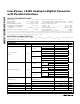
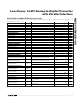
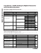
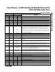
Pin Description
PIN NAME
MAX1165 MAX1166 MAX1165 MAX1166
FUNCTION
1 1 D8 D4/D12 Three-State Digital Data Output
2 2 D9 D5/D13 Three-State Digital Data Output
3 3 D10 D6/D14 Three-State Digital Data Output
4 4 D11 D7/D15 Three-State Digital Data Output. D15 is the MSB.
5 — D12 — Three-State Digital Data Output
6 — D13 — Three-State Digital Data Output
7 — D14 — Three-State Digital Data Output
8 — D15 — Three-State Digital Data Output (MSB)
95 R/C
Read/Convert Input. Power up and put the MAX1165/MAX1166 in acquisition mode
by holding R/C low during the first falling edge of CS. During the second falling
edge of CS, the level on R/C determines whether the reference and reference
buffer power down or remain on after conversion. Set R/C high during the second
falling edge of CS to power down the reference and buffer, or set R/C low to leave
the reference and buffer powered up. Set R/C high during the third falling edge of
CS to put valid data on the bus.
10 6 EOC End of Conversion. EOC drives low when conversion is complete.
11 7 AV
DD
Analog Supply Input. Bypass with a 0.1µF capacitor to AGND.
12 8 AGND Analog Ground. Primary analog ground (star ground).
13 9 AIN Analog Input
14 10 AGND
Analog Ground. Connect pin 14 to pin 12 (MAX1165). Connect pin 10 to pin 8
(MAX1166).
15 11 REFADJ
Refer ence Buffer Outp ut. Byp ass RE FAD J w i th a 0.1µF cap aci tor to AG N D for i nter nal
r efer ence m od e. C onnect RE FAD J to AV
D D
to sel ect exter nal r efer ence m od e.
16 12 REF
Reference Input/Output. Bypass REF with a 4.7µF capacitor to AGND for internal
reference mode. External reference input when in external reference mode.
17 — RESET Reset Input. Logic high resets the device.
— 13 HBEN
High-Byte Enable Input. Used to multiplex the 14-bit conversion result:
1: Most significant byte available on the data bus.
0: Least significant byte available on the data bus.
18 14 CS
Convert Start. The first falling edge of CS powers up the device and enables
acquire mode when R/C is low. The second falling edge of CS starts conversion.
The third falling edge of CS loads the result onto the bus when R/C is high.
19 15 DGND Digital Ground
20 16 DV
DD
Digital Supply Voltage. Bypass with a 0.1µF capacitor to DGND.
21 17 D0 D0/D8 Three-State Digital Data Output
22 18 D1 D1/D9 Three-State Digital Data Output
23 19 D2 D2/D10 Three-State Digital Data Output
24 20 D3 D3/D11 Three-State Digital Data Output
25 — D4 — Three-State Digital Data Output
26 — D5 — Three-State Digital Data Output
27 — D6 — Three-State Digital Data Output
28 — D7 — Three-State Digital Data Output