
Datasheet


MAX1165/MAX1166
Low-Power, 16-Bit Analog-to-Digital Converter
with Parallel Interface
2 _______________________________________________________________________________________
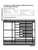
ABSOLUTE MAXIMUM RATINGS
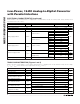
ELECTRICAL CHARACTERISTICS
(AV
DD
= DV
DD
= +5V, external reference = +4.096V, C
REF
= 4.7µF, C
REFADJ
= 0.1µF, T
A
= T
MIN
to T
MAX
, unless otherwise noted.
Typical values are at T
A
= +25°C.)
Stresses beyond those listed under “Absolute Maximum Ratings” may cause permanent damage to the device. These are stress ratings only, and functional
operation of the device at these or any other conditions beyond those indicated in the operational sections of the specifications is not implied. Exposure to
absolute maximum rating conditions for extended periods may affect device reliability.
AV
DD
to AGND .........................................................-0.3V to +6V
DV
DD
to DGND ........................................-0.3V to (AV
DD
+ 0.3V)
AGND to DGND.....................................................-0.3V to +0.3V
AIN, REF, REFADJ to AGND....................-0.3V to (AV
DD
+ 0.3V)
CS, HBEN, R/C, RESET to DGND ............................-0.3V to +6V
Digital Output (D15–D0, EOC)
to DGND ..............................................-0.3V to (DV
DD
+ 0.3V)
Maximum Continuous Current Into Any Pin ........................50mA
Continuous Power Dissipation (T
A
= +70°C)
20-Pin TSSOP (derate 10.9mW/°C above+70°C) ........879mW
28-Pin TSSOP (derate 12.8mW/°C above +70°C) .....1026mW
Operating Temperature Ranges
MAX116_ _CU_...................................................0°C to +70°C
MAX116_ _EU_ ................................................-40°C to +85°C
Storage Temperature Range .............................-65°C to +150°C
Junction Temperature......................................................+150°C
Lead Temperature (soldering, 10s) .................................+300°C
PARAMETER SYMBOL CONDITIONS MIN TYP MAX UNITS
DC ACCURACY
Resolution N 16 Bits
MAX116_A -2.5 +2.5
MAX116_B -2.5 +2.5
T
A
= -40°C
MAX116_C -4 +4
MAX116_A -2 +2
MAX116_B -2 +2
T
A
= 0°C
MAX116_C -4 +4
MAX116_A -2 +2
MAX116_B -2 +2
Relative Accuracy
(Note 1)
INL
T
A
= +85°C
MAX116_C -4 +4
LSB
MAX116_A -1 +2
No missing
codes
MAX116_B -1 +2
T
A
= -40°C
MAX116_C -2 +2
MAX116_A -1 +1.5
No missing
codes
MAX116_B -1 +1.5
T
A
= 0°C
MAX116_C -2 +2
MAX116_A -1 +1
No missing
codes
MAX116_B -1 +1.5
Differential Nonlinearity DNL
T
A
= +85°C
MAX116_C -2 +2
LSB
RMS noise, external reference, includes
quantization noise
0.65 LSB
RMS
Transition Noise
Internal reference 0.7 LSB
RMS
Offset Error 0.05 1 mV
Gain Error (Note 2) ±0.002 ±0.02 %FSR
Offset Drift 0.6 ppm/°C
Gain Drift 0.2 ppm/°C
DYNAMIC PERFORMANCE (f
IN(SINE-WAVE)
= 1kHz, V
IN
= 4.096V
P-P
, 165ksps)
Signal-to-Noise Plus Distortion SINAD 86 90 dB