
Datasheet


MAX11634–MAX11637
12-Bit, 300ksps ADCs with Differential
Track/Hold, and Internal Reference
10 ______________________________________________________________________________________
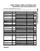
Pin Description
PIN
MAX11634
MAX11635
MAX11636
MAX11637
NAME FUNCTION
1–4 — AIN0–AIN3 Analog Inputs
5, 6 — N.C. No Connection. Not internally connected.
7 — REF- External Differential Reference Negative Input
8 — CNVST
Active-Low Conversion Start Input. See Table 3 for details on programming the
setup register.
9 9 REF+ Positive Reference Input. Bypass to GND with a 0.1µF capacitor.
10 10 GND Ground
11 11 V
DD
Power Input. Bypass to GND with a 0.1µF capacitor.
12 12 CS Active-Low Chip-Select Input. When CS is high, DOUT is high impedance.
13 13 SCLK
Serial-Clock Input. Clocks data in and out of the serial interface (duty cycle must
be 40% to 60%). See Table 3 for details on programming the clock mode.
14 14 DIN
Serial-Data Input. DIN data is latched into the serial interface on the rising edge of
SCLK.
15 15 DOUT
Serial-Data Output. Data is clocked out on the falling edge of SCLK. High
impedance when CS is connected to V
DD
.
16 16 EOC Active-Low End-of-Conversion Output. Data is valid after EOC pulls low.
— 1–6 AIN0–AIN5 Analog Inputs
— 7 REF-/AIN6
External Differential Reference Negative Input/Analog Input 6. See Table 3 for
details on programming the setup register.
— 8 CNVST/AIN7
Active-Low Conversion Start Input/Analog Input 7. See Table 3 for details on
programming the setup register.
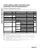
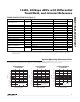
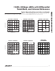
16
15
14
13
12
11
10
9
2
1
3
4
5
6
7
8
AIN0
( ) PINOUT FOR THE MAX11634/MAX11635.
TOP VIEW
EOC
DOUT
DIN
SCLK
CS
V
DD
GND
REF+
MAX11634–
MAX11637
QSOP
AIN1
AIN2
AIN5 (N.C.)
AIN3
AIN4 (N.C.)
REF-/AIN6 (REF-)
CNVST/AIN7 (CNVST)
+
Pin Configuration