
Datasheet


MAX11612–MAX11617
Low-Power, 4-/8-/12-Channel, I
2
C,
12-Bit ADCs in Ultra-Small Packages
4
Maxim Integrated
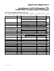
ELECTRICAL CHARACTERISTICS (continued)
(V
DD
= 2.7V to 3.6V (MAX11613/MAX11615/MAX11617), V
DD
= 4.5V to 5.5V (MAX11612/MAX11614/MAX11616), V
REF
= 2.048V
(MAX11613/MAX11615/MAX11617), V
REF
= 4.096V (MAX11612/MAX11614/MAX11616), f
SCL
= 1.7MHz, T
A
= T
MIN
to T
MAX
, unless
otherwise noted. Typical values are at T
A
= +25°C, see Tables 1–5 for programming notation.) (Note 1)
PARAMETER
SYMBOL
CONDITIONS
MIN TYP MAX
UNITS
POWER REQUIREMENTS
MAX11613/MAX11615/MAX11617 2.7 3.6
Supply Voltage V
DD
MAX11612/MAX11614/MAX11616 4.5 5.5
V
Internal reference
900 1150
f
SAMPLE
= 94.4ksps
external clock
External reference
670
900
Internal reference
530
f
SAMPLE
= 40ksps
internal clock
External reference
230
Internal reference
380
f
SAMPLE
= 10ksps
internal clock
External reference 60
Internal reference
330
f
SAMPLE
=1ksps
internal clock
External reference 6
Supply Current I
DD
Shutdown (internal REF off) 0.5 10
µA
Power-Supply Rejection Ratio PSRR Full-scale input (Note 10)
±0.5 ±2.0
LSB/V
TIMING CHARACTERISTICS (Figure 1)
(V
DD
= 2.7V to 3.6V (MAX11613/MAX11615/MAX11617), V
DD
= 4.5V to 5.5V (MAX11612/MAX11614/MAX11616), V
REF
= 2.048V
(MAX11613/MAX11615/MAX11617), V
REF
= 4.096V (MAX11612/MAX11614/MAX11616), f
SCL
= 1.7MHz, T
A
= T
MIN
to T
MAX
, unless
otherwise noted. Typical values are at T
A
= +25°C, see Tables 1–5 for programming notation.) (Note 1)
PARAMETER
SYMBOL
CONDITIONS
MIN TYP MAX
UNITS
TIMING CHARACTERISTICS FOR FAST MODE
Serial-Clock Frequency f
SCL
400 kHz
Bus Free Time Between a STOP (P)
and a START (S) Condition
t
BUF
1.3 µs
Hold Time for START (S) Condition
t
HD
,
STA
0.6 µs
Low Period of the SCL Clock t
LOW
1.3 µs
High Period of the SCL Clock t
HIGH
0.6 µs
Setup Time for a Repeated START
Condition (Sr)
t
SU
,
STA
0.6 µs
Data Hold Time (Note 11)
t
HD
,
DAT
0 900 ns
Data Setup Time
t
SU
,
DAT
100
ns
Rise Time of Both SDA and SCL
Signals, Receiving
t
R
Measured from 0.3V
DD
- 0.7V
DD
20 + 0.1C
B
300 ns
Fall Time of SDA Transmitting t
F
Measured from 0.3V
DD
- 0.7V
DD
(Note 12)
20 + 0.1C
B
300 ns
Setup Time for STOP (P) Condition
t
SU
,
STO
0.6 µs
Capacitive Load for Each Bus Line
C
B
400 pF
Pulse Width of Spike Suppressed
t
SP
50 ns