
Datasheet


MAX11606–MAX11611
Low-Power, 4-/8-/12-Channel, I
2
C,
10-Bit ADCs in Ultra-Small Packages
9
Maxim Integrated
Detailed Description
The MAX11606–MAX11611 analog-to-digital converters
(ADCs) use successive-approximation conversion tech-
niques and fully differential input track/hold (T/H) cir-
cuitry to capture and convert an analog signal to a
serial 12-bit digital output. The MAX11606/MAX11607
are 4-channel ADCs, the MAX11608/MAX11609 are
8-channel ADCs, and the MAX11610/MAX11611 are
12-channel ADCs. These devices feature a high-speed
2-wire serial interface supporting data rates up to
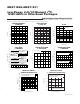
1.7MHz. Figure 2 shows the simplified internal structure
for the MAX11610/MAX11611.
Power Supply
The MAX11606–MAX11611 operates from a single sup-
ply and consumes 670µA (typ) at sampling rates up to
94.4ksps. The MAX11607/MAX11609/MAX11611 feature
a 2.048V internal reference and the MAX11606/
MAX11608/MAX11610 feature a 4.096V internal refer-
ence. All devices can be configured for use with an
external reference from 1V to V
DD
.
Analog Input and Track/Hold
The MAX11606–MAX11611 analog-input architecture
contains an analog-input multiplexer (mux), a fully dif-
ferential track-and-hold (T/H) capacitor, T/H switches, a
comparator, and a fully differential switched capacitive
digital-to-analog converter (DAC) (Figure 4).
In single-ended mode, the analog-input multiplexer con-
nects C
T/H
between the analog input selected by
CS[3:0] (see the
Configuration/Setup Bytes (Write
Cycle)
section) and GND (Table 3). In differential mode,
the analog- input multiplexer connects C
T/H
to the + and
- analog inputs selected by CS[3:0] (Table 4).
During the acquisition interval, the T/H switches are in
the track position and C
T/H
charges to the analog input
ANALOG
INPUT
MUX
AIN1
AIN11/REF
AIN2
AIN3
AIN4
AIN5
AIN6
AIN7
AIN8
AIN9
AIN10
AIN0
SCL
SDA
INPUT SHIFT REGISTER
SETUP REGISTER
CONFIGURATION REGISTER
CONTROL
LOGIC
REFERENCE
4.096V (MAX11610)
2.048V (MAX11611)
INTERNAL
OSCILLATOR
OUTPUT SHIFT
REGISTER
AND RAM
REF
T/H
10-BIT
ADC
V
DD
GND
MAX11610
MAX11611
Figure 2. MAX11610/MAX11611 Functional Diagram
V
DD
I
OL
I
OH
V
OUT
400pF
SDA
Figure 3. Load Circuit