
Datasheet

MAX11600–MAX11605
2.7V to 3.6V and 4.5V to 5.5V, Low-Power,
4-/8-/12-Channel 2-Wire Serial 8-Bit ADCs
20 ______________________________________________________________________________________
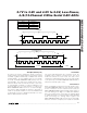
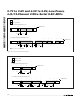
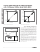
Layout, Grounding, and Bypassing
For best performance, use PC boards. Wire-wrap config-
urations are not recommended since the layout should
ensure proper separation of analog and digital traces. Do
not run analog and digital lines parallel to each other, and
do not lay out digital signal paths underneath the ADC
package. Use separate analog and digital PCB ground
sections with only one star point (Figure 14) connecting
the two ground systems (analog and digital). For lowest
noise operation, ensure the ground return to the star
ground’s power supply is low impedance and as short as
possible. Route digital signals far away from sensitive
analog and reference inputs.
High-frequency noise in the power supply (V
DD
) could
influence the proper operation of the ADC’s fast
comparator. Bypass V
DD
to the star ground with a
0.1µF capacitor located as close as possible to the
MAX11600–MAX11605 power-supply pin. Minimize
capacitor lead length for best supply-noise rejection,
and add an attenuation resistor (5Ω) if the power sup-
ply is extremely noisy.
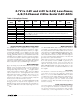
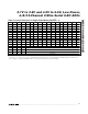
INPUT VOLTAGE (LSB)
OUTPUT CODE
1...111
1...110
1...101
1...100
0...000
0...001
0...010
0...011
23
256
V
REF
1 LSB =
1 253 255254
REF
2560 252
Figure 12. Unipolar Transfer Function
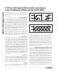
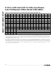
INPUT VOLTAGE (LSB)
OUTPUT CODE
(TWO'S COMPLEMENT)
0...111
0...110
0...101
0...100
1...000
1...001
1...010
1...011
-1-126 -125
256
V
REF
1 LSB =
0+1-127 +125 +127+126
0...000
0...001
1...111
REF
+128-128 +124
NEGATIVE INPUT
Figure 13. Bipolar Transfer Function
3V/5V
V
LOGIC
= 3V/5V
GND
SUPPLIES
DGND3V/5V
GND
0.1µF
V
DD
DIGITAL
CIRCUITRY
MAX11600–
MAX11605
R* = 5Ω
*OPTIONAL
Figure 14. Power-Supply and Grounding Connections