
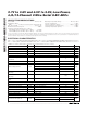
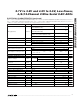
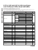
Datasheet


minimize sampling errors with higher source imped-
ances, connect a 100pF capacitor from the analog
input to GND. This input capacitor forms an RC filter
with the source impedance limiting the analog input
bandwidth. For larger source impedances, use a buffer
amplifier to maintain analog input signal integrity.
When operating in internal clock mode, the T/H circuitry
enters its tracking mode on the ninth falling clock edge
of the address byte (see the
Slave Address
section).
The T/H circuitry enters hold mode two internal clock
cycles later. A conversion or a series of conversions is
then internally clocked (eight clock cycles per conver-
sion) and the MAX11600–MAX11605 hold SCL low.
When operating in external clock mode, the T/H circuit-
ry enters track mode on the seventh falling edge of a
valid slave address byte. Hold mode is then entered on
the falling edge of the eighth clock cycle. The conver-
sion is performed during the next eight clock cycles.
The time required for the T/H circuitry to acquire an
input signal is a function of input capacitance. If the
analog input source impedance is high, the acquisition
time lengthens and more time must be allowed
between conversions. The acquisition time (t
ACQ
) is the
minimum time needed for the signal to be acquired. It is
calculated by:
t
ACQ
≥ 6.25 (R
SOURCE
+ R
IN
) C
IN
where R
SOURCE
is the analog input source impedance,
R
IN
= 2.5kΩ, and C
IN
= 18pF. t
ACQ
is 1/f
SCL
for external
clock mode. For internal clock mode, the acquisition
time is two internal clock cycles. To select R
SOURCE
,
allow 625ns for t
ACQ
in internal clock mode to account
for clock frequency variations.
MAX11600–MAX11605
2.7V to 3.6V and 4.5V to 5.5V, Low-Power,
4-/8-/12-Channel 2-Wire Serial 8-Bit ADCs
_______________________________________________________________________________________ 9
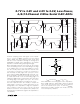
t
HD.STA
t
SU.DAT
t
HIGH
t
R
t
F
t
HD.DAT
t
HD.STA
S
Sr
A
SCL
SDA
t
SU.STA
t
LOW
t
BUF
t
SU.STO
PS
t
HD.STA
t
SU.DAT
t
HIGH
t
FCL
t
HD.DAT
t
HD.STA
S Sr A
SCL
SDA
t
SU.STA
t
LOW
t
BUF
t
SU.STO
S
t
RCL
t
RCL1
HS MODE F/S MODE
a) F/S-MODE I
2
C SERIAL-INTERFACE TIMING
b) HS-MODE I
2
C SERIAL-INTERFACE TIMING
t
FDA
t
RDA
t
t
R
t
F
Figure 1. I
2
C Serial-Interface Timing
V
DD
I
OL
= 3mA
I
OH
= 0mA
V
OUT
400pF
SDA
Figure 2. Load Circuit