
Datasheet

Detailed Description
Converter Operation
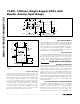
The MAX1157/MAX1159/MAX1175 use a successive-
approximation (SAR) conversion technique with an
inherent track-and-hold (T/H) stage to convert an analog
input into a 14-bit digital output. Parallel outputs provide
a high-speed interface to microprocessors (µPs). The
Functional Diagram at the end of the data sheet shows a
simplified internal architecture of the MAX1157/
MAX1159/MAX1175. Figure 3 shows a typical applica-
tion circuit for the MAX1157/MAX1159/MAX1175.
Analog Input
Input Scaler
The MAX1157/MAX1159/MAX1175 have an input scaler
which allows conversion of true bipolar input voltages
and input voltages greater than the power supply, while
operating from a single +5V analog supply. The input
scaler attenuates and shifts the analog input to match
the input range of the internal DAC. The MAX1157 has
a unipolar input voltage range of 0 to +10V. The
MAX1175 input voltage range is ±5V while the
MAX1159 input voltage range is ±10V. Figure 4 shows
the equivalent input circuit of the MAX1157/
MAX1159/MAX1175. This circuit limits the current going
into or out of AIN to less than 1.8mA.
MAX1157/MAX1159/MAX1175
14-Bit, 135ksps, Single-Supply ADCs with
Bipolar Analog Input Range
_______________________________________________________________________________________ 7
Pin Description (continued)
PIN NAME FUNCTION
15 REFADJ
Reference Buffer Output. Bypass REFADJ with a 0.1µF capacitor to AGND for internal reference
mode. Connect REFADJ to AV
DD
to select external reference mode.
16 REF
Reference Input/Output. Bypass REF with a 10µF capacitor to AGND. REF is the external reference
input when in external reference mode.
17 RESET Reset Input. Logic high resets the device.
18 CS
Convert Start. The first falling edge of CS powers up the device and enables acquisition when R/C
is low. The second falling edge of CS starts conversion. The third falling edge of CS loads the result
onto the bus when R/C is high.
19 DGND Digital Ground
20 DV
DD
Digital Supply Voltage. Bypass with a 0.1µF capacitor to DGND.
21, 22 N.C. No Connection. Make no connection to these pins.
23 D0 Three-State Digital Data Output (LSB)
24 D1 Three-State Digital Data Output
25 D2 Three-State Digital Data Output
26 D3 Three-State Digital Data Output
27 D4 Three-State Digital Data Output
28 D5 Three-State Digital Data Output
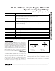
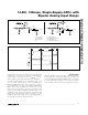
Figure 1. Load Circuits
1mA
DGND
HIGH-Z TO V
OH
,
V
OL
TO V
OH
, AND
V
OH
TO HIGH-Z
C
LOAD
= 20pF
D0–D13
A)
1mA
DV
DD
DGND
HIGH-Z TO V
OL
,
V
OH
TO V
OL
, AND
V
OL
TO HIGH-Z
C
LOAD
= 20pF
D0–D13
B)