
Datasheet

MAX1157/MAX1159/MAX1175
14-Bit, 135ksps, Single-Supply ADCs with
Bipolar Analog Input Range
2 _______________________________________________________________________________________
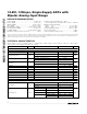
ABSOLUTE MAXIMUM RATINGS
Stresses beyond those listed under “Absolute Maximum Ratings” may cause permanent damage to the device. These are stress ratings only, and functional
operation of the device at these or any other conditions beyond those indicated in the operational sections of the specifications is not implied. Exposure to
absolute maximum rating conditions for extended periods may affect device reliability.
AV
DD
to AGND .........................................................-0.3V to +6V
DV
DD
to DGND.........................................................-0.3V to +6V
AGND to DGND.....................................................-0.3V to +0.3V
AIN to AGND .....................................................-16.5V to +16.5V
REF, REFADJ to AGND............................-0.3V to (AV
DD
+ 0.3V)
CS, R/C, RESET to DGND ........................................-0.3V to +6V
D_, EOC to DGND ...................................-0.3V to (DV
DD
+ 0.3V)
Maximum Continuous Current Into Any Pin ........................50mA
Continuous Power Dissipation (T
A
= +70°C)
28-Pin TSSOP (derate 12.8mW/°C above +70°C) .....1026mW
Operating Temperature Range
MAX11_ _ _CUI...................................................0°C to +70°C
MAX11_ _ _EUI ................................................-40°C to +85°C
Storage Temperature Range .............................-65°C to +150°C
Junction Temperature......................................................+150°C
Lead Temperature (soldering, 10s) .................................+300°C
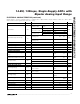
ELECTRICAL CHARACTERISTICS
(AV
DD
= DV
DD
= +5V ±5%, external reference = +4.096V, C
REF
= 10µF, C
REFADJ
= 0.1µF, V
REFADJ
= AV
DD
, T
A
= T
MIN
to T
MAX
,
unless otherwise noted. Typical values are at T
A
= +25°C.)
PARAMETER SYMBOL CONDITIONS MIN TYP MAX UNITS
DC ACCURACY
Resolution RES 14 Bits
Differential Nonlinearity DNL No missing codes over temperature -1 +1 LSB
MAX11_ _A -1 +1
Integral Nonlinearity INL
MAX11_ _B -2 +2
LSB
RMS noise, external reference 0.32
Transition Noise
Internal reference 0.34
LSB
RMS
MAX1159 -10 0 +10
Offset Error
MAX1157/MAX1175 -10 +10
mV
Gain Error 0 ±0.2 %FSR
Offset Drift 16 µV/°C
Gain Drift ±1 ppm/°C
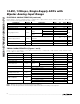
AC ACCURACY (f
IN
= 1kHz, V
AIN
= full range, 135ksps)
Signal-to-Noise Plus Distortion SINAD 81 85 dB
Signal-to-Noise Ratio SNR 82 85 dB
Total Harmonic Distortion THD -100 -86 dB
Spurious-Free Dynamic Range SFDR 87 103 dB
ANALOG INPUT
MAX1157 0 +10
MAX1159 -10 +10
Input Range V
AIN
MAX1175 -5 +5
V
MAX1157/MAX1175 Normal operation 5.3 6.9 9.2
MAX1175 Shutdown mode 3
MAX1157 Shutdown mode 5.3
Normal operation 7.8 10 13.0
Input Resistance R
AIN
MAX1159
Shutdown mode 6
kΩ