
Datasheet


MAX1146–MAX1149
Multichannel, True-Differential,
Serial, 14-Bit ADCs
18 ______________________________________________________________________________________
Shutdown and Power-Down Modes
The MAX1146–MAX1149 provide a hardware shutdown
and two software power-down modes.
Pulling SHDN low places the converter in hardware
shutdown. The conversion is immediately terminated
and the supply current is reduced to 300nA. Allow 2ms
for the device to power-up when the internal reference
buffer is used with C
REFADJ
= 0.01µF and C
REF
=
2.2µF. Larger capacitors on C
REFADJ
and C
REF
increase the power-up time (Table 6). No wake-up time
is needed for the device to power-up from fast power-
down when using an external reference.
Select a software power-down mode through the PD1
and PD0 bits of the control byte (Table 1). When the
conversion in progress is complete, software power-
down is initiated. The serial interface remains active
and the last conversion result can be clocked out. In
full power-down mode, only the serial interface remains
operational and the supply current is reduced to
300nA. In fast power-down mode, only the bandgap
reference and the serial interface remain operational,
and the supply current is reduced to 600µA.
The MAX1146–MAX1149 automatically wake up from
software power-down when they receive the control
byte’s start bit (Table 1). Allow 2ms for the device to
power-up when the internal reference buffer is used
with C
REFADJ
= 0.01µF and C
REF
= 2.2µF. Larger
capacitors on C
REFADJ
and C
REF
increase the power-
up time (Table 6). No wake-up time is needed for the
device to power-up from fast power-down when using
an external reference.
Reference Voltage
The MAX1146–MAX1149 can be used with an internal
or external reference voltage. The reference voltage
determines the ADC input range. The reference deter-
mines the full-scale output value (Table 7).
Internal Reference
The MAX1146–MAX1149 contain an internal 1.250V
bandgap reference. This bandgap reference is connect-
ed to REFADJ through a 20kΩ resistor. Bypass REFADJ
with a 0.01µF capacitor to AGND. The MAX1146/
MAX1148 reference buffer has a 3.277V/V gain to pro-
vide +4.096V at REF. The MAX1147/MAX1149 reference
buffer has a 2.000V/V gain to provide +2.500V at REF.
Bypass REF with a minimum 2.2µF capacitor to AGND
when using the internal reference.
External Reference
An external reference can be applied to the
MAX1146–MAX1149 in two ways:
1) Disable the internal reference buffer by connecting
REFADJ to V
DD
and apply the external reference to
REF (Figure 12).
2) Utilize the internal reference buffer by applying an
external reference to REFADJ (Figure 13).
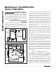
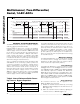
SCLK
SSTRB
DIN
START
SEL2 SEL1
SEL0
PD1
PD0
18
INPUT MUX
INPUT T/H
SET ACCORDING TO PREVIOUS
CONTROL BYTE
TRACK HOLD
t
CONV
t
CONV
DOUT
HIGH-Z
t
ACQ
14
TRACK
D13 D12
10 18
D5 D4 D3 D2 D1 D0
11
HOLD
14
D13 D12
START
10
D5 D4
SEL2
11
TRACK
CB1 CB2
SET TO CB2SET TO CB1
RESET TO CB1
OPEN RESET TO CB2OPEN
CS
START
SEL2 SEL1
SEL0
PD1
PD0
SGL/DIF
UNI/BIP
SGL/DIF
UNI/BIP
t
ACQ
Figure 11. Internal Clock Mode—18 Clocks/Conversion Timing
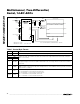
C
REFADJ
*
C
REF
POWER-UP TIMES FROM AN
EXTENDED POWER-DOWN
0.01µF 4.7µF 2ms
0.1µF 10µF 25ms
Table 6. Internal Reference Buffer Power-
Up Times vs. Bypass Capacitors
*Power-up times are dominated by C
REFADJ
.