
Datasheet


MAX1146–MAX1149
Multichannel, True-Differential,
Serial, 14-Bit ADCs
14 ______________________________________________________________________________________
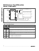
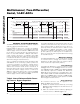
BIT NAME DESCRIPTION
7 (MSB)
START
Start bit. The first logic 1 bit after CS goes low defines the beginning of the control byte.
6 SEL2
5 SEL1
4 SEL0
Channel-select bits. The channel-select bits select which of the eight channels are used for the conversion
(Tables 2, 3, 4, and 5).
3
SGL/DIF
1 = single ended, 0 = differential. Selects single-ended or differential conversions. In single-ended mode,
input signal voltages are referred to COM. In differential mode, the voltage difference between two channels
is measured.
2
UNI/BIP
1 = unipolar, 0 = bipolar. Selects unipolar or bipolar conversion mode. In unipolar mode, connect COM to
AGND to perform conversion from 0 to V
REF
. In bipolar mode, connect COM to V
REF
/2 to perform conversion
from 0 to V
REF
. See Table 7.
1 PD1
0 (LSB)
PD0
Selects clock and power-down modes.
PD1 = 0 and PD0 = 0 selects full power-down mode*.
PD1 = 0 and PD0 = 1 selects fast power-down mode*.
PD1 = 1 and PD0 = 0 selects internal clock mode.
PD1 = 1 and PD0 = 1 selects external clock mode.
Table 1. Control Byte Format
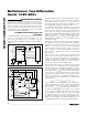
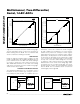
MAX1148
MAX1149
OSCILLOSCOPE
CH1 CH2 CH3 CH4
*FULL-SCALE ANALOG INPUT, CONVERSION RESULT = $FFF HEX
SCLK
SSTRB
DOUT*
DOUT
SSTRB
SCLK
DIN
V
DD
DGND
AGND
COM
0.01µF
0.01µF
2.2µF
EXTERNAL CLOCK
CH7
REFADJ
REF
MAX1149 V
REF
= +2.500V
MAX1148 V
REF
= +4.096V
V
REF
A
IN
V
DD
10Ω
10Ω
V
COM
≤ A
IN
≤ V
REF
SHDN
CS
0.1µF 4.7µF
Figure 7. Quick-Look Circuit
*The start bit resets power-down modes.