
Datasheet


MAX1136–MAX1139
10ms prior to conversion or powered continuously.
Wake-up is invisible when using an external reference or
V
DD
as the reference.
Automatic shutdown results in dramatic power savings,
particularly at slow conversion rates and with internal
clock. For example, at a conversion rate of 10ksps, the
average supply current for the MAX1137 is 60µA (typ) and
drops to 6µA (typ) at 1ksps. At 0.1ksps the average sup-
ply current is just 1µA, or a minuscule 3µW of power con-
sumption, see Average Supply Current vs. Conversion
Rate in the
Typical Operating Characteristics
.
Reference Voltage
SEL[2:0] of the setup byte (Table 1) control the reference
and the AIN_/REF configuration (Table 6). When AIN_/REF
is configured to be a reference input or reference output
(SEL1 = 1), differential conversions on AIN_/REF appear
as if AIN_/REF is connected to GND (see Note 2 and
Table 4). Single-ended conversion in scan mode on
AIN_/REF will be ignored by internal limiter, which sets the
highest available channel at AIN2 or AIN10.
Internal Reference
The internal reference is 4.096V for the MAX1136/
MAX1138 and 2.048V for the MAX1137/MAX1139. SEL1
of the setup byte controls whether AIN_/REF is used for an
analog input or a reference (Table 6). When AIN_/REF is
configured to be an internal reference output (SEL[2:1] =
11), decouple AIN_/REF to GND with a 0.1µF capacitor
and a 2kΩ sereis resistor (see the
Typical Operating
Circuit
). Once powered up, the reference always remains
on until reconfigured. The internal reference requires 10ms
to wake up and is accessed using SEL0 (Table 6). When
in shutdown, the internal reference output is in a high-
impedance state. The reference should not be used to
supply current for external circuitry. The internal reference
does not require an external bypass capacitor and works
best when not connected to the pin (SEL1 = 0).
External Reference
The external reference can range from 1V to V
DD
. For
maximum conversion accuracy, the reference must be
able to deliver up to 40µA and have an output imped-
ance of 500Ω or less. If the reference has a higher out-
put impedance or is noisy, bypass it to GND as close to
AIN_/REF as possible with a 0.1µF capacitor.
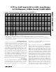
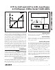
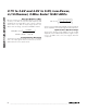
Transfer Functions
Output data coding for the MAX1136–MAX1139 is bina-
ry in unipolar mode and two’s complement in bipolar
mode with 1 LSB = (V
REF
/2N) where ‘N’ is the number
of bits (10). Code transitions occur halfway between
successive-integer LSB values. Figure 12 and Figure
13 show the input/output (I/O) transfer functions for
unipolar and bipolar operations, respectively.
Layout, Grounding, and Bypassing
Only use PC boards. Wire-wrap configurations are not
recommended since the layout should ensure proper
separation of analog and digital traces. Do not run ana-
log and digital lines parallel to each other, and do not
layout digital signal paths underneath the ADC pack-
2.7V to 3.6V and 4.5V to 5.5V, Low-Power,
4-/12-Channel, 2-Wire Serial 10-Bit ADCs
18 ______________________________________________________________________________________
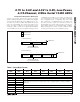
SEL2 SEL1 SEL0 REFERENCE VOLTAGE AIN_/REF
INTERNAL REFERENCE
STATE
00X V
DD
Analog Input Always Off
0 1 X External Reference Reference Input Always Off
1 0 0 Internal Reference Analog Input Always Off
1 0 1 Internal Reference Analog Input Always On
1 1 0 Internal Reference Reference Output Always Off
1 1 1 Internal Reference Reference Output Always On
Table 6. Reference Voltage and AIN_/REF Format
OUTPUT CODE
FULL-SCALE
TRANSITION
11 . . . 111
11 . . . 110
11 . . . 101
00 . . . 011
00 . . . 010
00 . . . 001
00 . . . 000
123
0
FS
FS - 3/2 LSB
FS = V
REF
ZS = GND
INPUT VOLTAGE (LSB)
1 LSB =
V
REF
1024
MAX1136–
MAX1139
Figure 12. Unipolar Transfer Function